
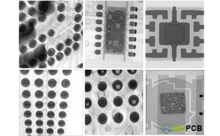
In the field of renewable energy, inverters serve as the core hub connecting power generation units to the grid. Their performance, reliability, and safety directly determine the efficiency and return on investment of the entire system. These devices must operate stably for extended periods under harsh high-voltage and high-current conditions, placing unprecedented demands on their internal printed circuit boards (PCBs). To address these challenges, a comprehensive and precise quality control system is essential, and SPI/AOI/X-Ray inspection forms the foundation of this system. It is not merely a defect detection tool but a critical safeguard that spans the entire product lifecycle—from design validation to mass production—ensuring power connections, thermal management, and electrical performance meet the highest standards.
As grid-tie and safety compliance engineers, we understand that even the slightest manufacturing flaw, such as solder voids, connector cold joints, or busbar contact issues, can escalate into catastrophic failures under high-power loads, leading to equipment downtime or even safety incidents. Therefore, this article examines how SPI/AOI/X-Ray inspection fundamentally addresses key challenges in inverter PCB manufacturing, including busbar-to-terminal connections, crimping and soldering process consistency, and EMI-thermal co-design, ensuring every PCB leaving the factory can confidently handle high-voltage and high-current demands. We will analyze how these advanced inspection technologies integrate with the NPI EVT/DVT/PVT phases to provide robust data support for the product's exceptional performance.
Busbars and Terminals: Contact Resistance, Thermal Effects, and Assembly Robustness
The core function of renewable energy inverters is to handle kilowatt to megawatt-level power, which means PCBs must carry hundreds of amperes of current. Traditional copper traces are no longer sufficient, replaced instead by heavy copper foils, embedded busbars, and high-specification terminals. The quality of these power interconnect components directly impacts two critical system metrics: efficiency and reliability.
First, any connection point exhibits contact resistance. According to Joule’s Law (P = I²R), even milliohm-level contact resistance under hundred-ampere currents generates significant power loss, dissipated as heat. This additional heat, or thermal rise, is one of the most challenging aspects of inverter PCB design. Excessive thermal rise accelerates component aging, reduces system efficiency, and can even melt connection points, potentially causing fires.
SPI/AOI/X-Ray inspection plays an irreplaceable role in this context:
- AOI (Automated Optical Inspection): For bolted busbars or crimped terminals, AOI rapidly checks assembly accuracy, including position, orientation, full seating, and fastener presence. It ensures mechanical connection robustness, laying the foundation for subsequent electrical performance.
- X-Ray Inspection: For large terminals or embedded busbars soldered to PCBs, the internal quality of solder joints is critical to contact resistance. X-Ray penetrates components to clearly reveal solder joint structures, precisely identifying and quantifying void ratios. Solder voids significantly reduce current pathway cross-sections, leading to localized current density spikes and increased contact resistance. By enforcing strict void ratio standards (e.g., IPC-A-610) and employing 100% or sampling X-Ray inspections, manufacturers can eliminate hotspots caused by poor soldering at the source. For complex THT/through-hole soldering connections, X-Ray is the only reliable method to verify hole fill rates and solder joint integrity. During the First Article Inspection (FAI) phase of the product, we use X-Ray to conduct a thorough analysis of the critical power connection points of the first article, establishing a gold standard. This First Article Inspection (FAI) report, which includes detailed X-Ray images and data, is the benchmark for setting up AOI and X-Ray procedures in subsequent mass production, ensuring consistency across all products. HILPCB has extensive experience in handling Heavy Copper PCBs, seamlessly integrating advanced inspection technologies with manufacturing processes to ensure every high-current connection point is as solid as a rock.
Crimping and Soldering Processes: Defining Process Windows and Achieving Consistency Validation
A reliable electrical connection stems from a stable and controlled manufacturing process. For power connections in inverter PCBs, the primary methods involve crimping and soldering. SPI/AOI/X-Ray inspection provides closed-loop quality monitoring for these processes, ensuring they always operate within the optimal process window.
Consistency Validation for Crimping Processes:
Crimping is a process where terminals and wires are tightly bonded through mechanical deformation. A perfect crimp should form an airtight cold-weld connection internally, with extremely low resistance and excellent mechanical strength. However, crimp quality is influenced by factors such as crimp height, tool wear, and operator technique. Traditional validation methods involve destructive cross-sectional analysis, which is costly and unsuitable for mass production. While AOI can inspect the external appearance of crimps, such as the bell-mouth shape and wire protrusion length, it cannot assess internal compaction. Here, high-resolution X-Ray inspection, though not commonly used, can non-destructively observe the deformation of internal wire strands during critical applications or failure analysis, aiding in crimp quality assessment. More importantly, during the NPI EVT/DVT/PVT phases, rigorous pull-force testing and cross-sectional analysis of crimped samples, combined with AOI data, can precisely define a robust process window.
Precision Control for Soldering Processes:
Soldering is the core of inverter PCB assembly. Especially for complex boards with mixed SMT and through-hole components, the selection and control of soldering processes are critical.
- SPI (Solder Paste Inspection): For large SMT components like power MOSFETs and IGBT modules mounted on PCBs, the soldering quality of their thermal pads directly impacts heat dissipation efficiency. SPI conducts 3D inspection immediately after solder paste printing, precisely measuring the volume, area, height, and offset of the solder paste. This ensures sufficient and uniform solder for subsequent reflow soldering, preventing cold joints and poor heat dissipation due to insufficient solder paste at the source.
- Selective Wave Soldering: For high-density through-hole components like large capacitors, inductors, and connectors, Selective Wave Soldering is an ideal process. It precisely targets specific areas for soldering, avoiding impact on adjacent SMT components. However, its process parameters (nozzle type, soldering time, nitrogen flow rate, etc.) must be precisely controlled. AOI and X-Ray form a perfect combination here. AOI inspects the surface wettability, shape, and defects like bridging or solder balls, while X-Ray delves deeper to check whether through-hole solder fill meets IPC standards (typically >75%) and identifies hidden internal shorts or voids. Through continuous monitoring of the Selective Wave Soldering process, high quality and reliability for THT/through-hole soldering can be ensured. At HILPCB, we provide highly consistent and reliable soldering quality for our customers through a rigorous Through-Hole Assembly process, combined with online SPI, AOI, and offline X-Ray inspections.
Inverter PCB Critical Connection Point Inspection Process
- Design Phase (DFM/DFA): Collaborate with customers to optimize busbar, terminal, and heavy copper layouts, ensuring manufacturability and inspectability. Evaluate thermal paths and EMI shielding requirements.
- NPI EVT/DVT/PVT Phases:
- Conduct comprehensive First Article Inspection (FAI) to establish inspection benchmarks.
- Perform electrical characteristic verification using Flying probe test to ensure no open or short circuits.
- Conduct cross-sectional analysis of critical solder joints via X-Ray, optimizing Selective wave soldering and reflow soldering process parameters.
- Solder Paste Printing (SMT): 100% online SPI inspection to monitor solder paste printing quality and prevent soldering defects.
- Post Reflow/Selective Wave Soldering:
- 100% online AOI inspection to check component placement, solder joint appearance, polarity, etc.
- Perform batch X-Ray inspection on BGA, QFN, and critical power device solder joints, focusing on void rate and internal defects.
- Final Assembly and Testing: Functional testing (FCT) and aging testing, combined with traceable inspection data, ensure final product quality.
EMI and Thermal Management Co-Design for High-Current Paths
In inverters, the high-current paths with high-frequency switching are not only the primary heat sources but also strong sources of electromagnetic interference (EMI). Effective thermal management and EMI control are critical to ensuring stable inverter operation and compliance with grid-connected safety certifications. PCB design itself is the core of their interaction, and SPI/AOI/X-Ray inspection is the key tool to verify whether the design intent is perfectly realized during manufacturing.
Verification of Thermal Management Path Integrity:
Modern inverter PCBs widely adopt High-Thermal PCB materials and designs, such as large copper planes, arrays of thermal vias, and exposed copper areas directly contacting heat sinks. These designs aim to provide power devices with a low-thermal-resistance heat dissipation path.
- AOI plays a role here by inspecting the surface integrity of these critical features. For example, it can verify whether thermal vias are accidentally covered by solder mask or if exposed copper areas have scratches or contamination, which could severely impact thermal performance.
- X-Ray goes deeper. For thermal vias buried between layers or covered by large components, X-Ray can inspect the uniformity and integrity of their internal plating. More importantly, for power devices (such as TO-247 or LGA-packaged power modules) directly soldered to PCB thermal pads, the void rate of solder joints directly determines thermal resistance. A solder joint filled with voids significantly reduces thermal conductivity. By precisely measuring void percentages with X-Ray and comparing them against design specifications, products with potential thermal risks can be effectively screened out.
Manufacturing Assurance for EMI Control Designs:
To suppress EMI, designers employ methods like grounding shields, filter circuits, and controlled loop areas. The realization of these designs also relies on precise manufacturing.
- High-Speed Signal Integrity: The frequency of inverter control signals (e.g., PWM drive signals) is increasing, demanding stricter impedance control for traces. AOI can accurately measure trace width and spacing to ensure compliance with impedance design requirements, thereby reducing signal reflection and crosstalk and lowering EMI.
- Ground Connection Reliability: A low-impedance, continuous ground plane is the foundation of EMI shielding. X-Ray can inspect the soldering quality of critical ground vias and the reliability of ground layer connections in multilayer boards, preventing EMI leakage due to poor grounding. During early NPI EVT/DVT/PVT stages, Flying probe tests can quickly verify the correctness of all network connections, including complex grounding networks, providing confidence for subsequent EMI testing.
By translating design requirements into specific, measurable manufacturing metrics and systematically verifying them with SPI/AOI/X-Ray inspection, HILPCB ensures that the synergistic effects of thermal management and EMI control designs are faithfully reflected on every PCB.
Reliability and Maintainability: Connectors, Terminal Replacement, and Full Lifecycle Considerations
Renewable energy equipment is typically designed for a lifespan of 20-25 years, meaning its internal components must exhibit extremely high long-term reliability while accounting for maintainability throughout their lifecycle. SPI/AOI/X-Ray inspection not only guarantees initial product quality at the factory but also provides critical data for assessing long-term reliability and guiding field maintenance.
The Foundation of Long-Term Reliability: Inverters undergo frequent thermal cycling and mechanical vibrations during operation. Solder joints that exhibit micro-cracks or excessive voiding in initial X-Ray inspections, even if they pass factory functional tests, are highly likely to fail under prolonged stress. Therefore, screening out these potential "time bombs" during the manufacturing phase through rigorous SPI/AOI/X-Ray inspection is the first and most critical line of defense for ensuring long-term reliability. Particularly for heavy components in THT/through-hole soldering, the mechanical strength and fatigue resistance of solder joints are critical, making X-Ray inspection a key method for evaluating long-term reliability.
Design for Maintainability and Consistency:
During an inverter's lifecycle, certain components (e.g., fans, capacitors, connectors) may require replacement. Design must account for the replaceability of these parts. For instance, using highly reliable crimped or bolted connectors instead of direct soldering.
- AOI can verify proper connector installation and latch engagement at this stage, ensuring field technicians can easily plug/unplug without damaging the PCB.
- For soldered components requiring field replacement, original manufacturing data becomes especially critical. A comprehensive First Article Inspection (FAI) report, including X-Ray images and process parameters of the original solder joints, provides precise guidance for repairs, ensuring replacement parts meet the same quality standards as factory-original ones.
HILPCB's Turnkey Assembly Service not only focuses on initial manufacturing success but also considers the product's entire lifecycle. By establishing a comprehensive inspection database, we support the long-term reliability and maintainability of customer products.
Key Points for Inverter PCB Inspection
- ✅Power Path Integrity: Use X-Ray to inspect voiding rates in busbars, terminals, and heavy copper foil solder joints, ensuring low contact resistance and superior current-carrying capacity.
- ✅Thermal Management Effectiveness: Validate manufacturing quality of thermal vias and heat dissipation pads through AOI and X-Ray, ensuring efficient heat transfer from power devices.
Full-process Inspection and Traceability: Data-driven Decision Making from NPI to Mass Production
In modern electronics manufacturing, SPI/AOI/X-Ray inspection is no longer isolated inspection stations but intelligent nodes integrating data collection, analysis, and feedback functions, providing data-driven decision support throughout the entire process from New Product Introduction (NPI) to mass production.
Process Optimization in NPI Phase: During the NPI EVT/DVT/PVT stages, the goal is rapid iteration to validate designs and stabilize processes.
- EVT (Engineering Verification Test): At this stage with minimal yield, Flying probe test is typically used for rapid electrical verification to confirm circuit connectivity without expensive test fixtures. Meanwhile, engineers conduct detailed analysis using AOI and X-Ray on samples to identify potential design or early-stage process issues.
- DVT (Design Verification Test): Designs become more stable, and small-batch trial production begins. This is the critical period for comprehensive First Article Inspection (FAI). Through thorough SPI, AOI, and X-Ray inspections of first articles, cross-referenced with design documents (such as BOM and Gerber files, which can be checked using tools like BOM Viewer), all manufacturing and inspection parameters can be finalized.
- PVT (Production Verification Test): The final production line verification before mass production. At this point, all automated inspection programs are debugged, and the production line operates at mass production tempo. Collected SPI, AOI, and X-Ray data are used to evaluate process stability and repeatability (Cpk), ensuring quality for mass production.
Process Control and Traceability in Mass Production: During mass production, inspection systems shift from "problem detection" to "problem prevention." If SPI systems continuously detect solder paste misalignment, they automatically alert the upstream stencil printer for cleaning. If AOI identifies increased placement defects for specific components, it can trace back to particular pick-and-place nozzles. X-Ray void rate data can be correlated with reflow soldering temperature profiles to optimize thermal settings.
This real-time Statistical Process Control (SPC) capability is core to modern high-quality manufacturing. More importantly, all inspection data (images, measurements, defect classifications) are bound to each PCB's unique serial number, forming a complete production history. Should any issues arise later—whether customer complaints or field failures—the serial number enables rapid tracing of all inspection data for that board, significantly improving root cause analysis efficiency and accuracy.