
Tabbed routing adds periodic copper features to traces where a dense DDR breakout restricts line width and spacing. A suitable geometry can change impedance and reduce far-end crosstalk (FEXT), but it can also change delay, loss and other coupling. Evaluate the actual stackup and channel before choosing it.
For the broader decisions on topology, termination and timing, see our DDR PCB layout checklist. The discussion here focuses on whether a tabbed section is useful and how to verify it.
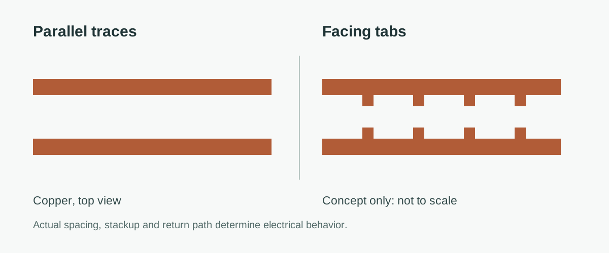
1. When Should You Consider Tabs?
In a BGA escape, available trace width, spacing and reference geometry may differ from the open routing region. A narrow section can have a different impedance, while nearby nets can couple to each other. The impact depends on the length and transitions as well as the complete channel.
Before adding tabs, compare the original route with practical alternatives: shorten the constrained run, change layers or escape geometry, adjust the stackup, or increase spacing where possible. A tabbed layout is a candidate when the constrained section still materially affects the design and there is room to manufacture and model the added copper. Neither a DIMM nor a chip-down topology alone determines the answer.
| Decision | Compare or check | Evidence for the choice |
|---|---|---|
| Constrained escape | Untabbed section and feasible routing alternatives | Actual geometry, reference path and channel simulation |
| Tab geometry | Width, length, pitch and clearance to all neighboring nets | Extracted model over the relevant frequency range |
| Signal timing | Each affected path, including DQ and its associated strobe | Applicable component guidance and system timing budget |
| Fabrication | Copper thickness, spacing, etch compensation and CAM handling | Fabricator review of the released design |
| Acceptance | Test structure, method and limits | Agreement on coupon representativeness and deliverables |
2. How Can Tabs Change Impedance and Crosstalk?
Adding copper changes the electromagnetic field around a trace. Depending on the geometry, it can increase capacitance and change both self and mutual inductance and capacitance. Those changes affect impedance, propagation and coupling together. A field solver or suitable extracted model should include the reference conductors, nearby nets, transitions and the frequency range relevant to the edge rate.
FEXT is the coupled disturbance observed at the far end of a victim line. Tabs may improve the balance of electric and magnetic coupling for a particular geometry, but adding mutual capacitance alone does not guarantee improvement. Near-end crosstalk, insertion loss and other neighboring nets also need checking. Ideal homogeneous stripline can have low FEXT, while practical structures can differ because of asymmetry, transitions and other nonidealities.
Song and coauthors, Electronics 10 (2021), 1590, DOI 10.3390/electronics10131590, compared manufactured tabbed microstrip test structures, measurements and models. Their work shows that both inductance and capacitance change and that results depend on the chosen dimensions. Its measurements and simulations apply to those test structures; they are not an acceptance limit or a prediction for another DDR board.
3. A Bounded Impedance and Delay Example
For an ideal, uniform, lossless single-mode line, impedance is Z0 = sqrt(L/C) and delay per unit length is td = sqrt(L*C). As an arithmetic illustration only, assume the effective inductance per unit length stays fixed while capacitance changes enough to move the ideal impedance from 52 Ω to 40 Ω:
C2/C1 = (52/40)² = 1.69 and td2/td1 = sqrt(1.69) = 1.30.
If the original delay is assumed to be 5.7 ps/mm, the same model gives 7.41 ps/mm after the change. The increase is approximately 17 ps over 10 mm or 34 ps over 20 mm. These are hypothetical numbers, not measured tab delays or a typical penalty.
Real tabs change geometry and can change inductance, coupling and frequency response as well. A short pitch alone does not prove that the structure behaves as a uniform line across the required bandwidth. Extract or simulate the actual periodic section and its transitions; use the resulting channel response to assess impedance, crosstalk and delay.
4. How Should DDR Timing Be Checked?
An equal physical length does not necessarily mean equal propagation delay when different segments have different geometries. Include the tabbed and untabbed portions, vias, packages and other relevant channel elements in the timing assessment, using the endpoint and measurement definitions required by the controller and memory documentation.
Compare the extracted delays of each affected net with the applicable setup, hold and skew budget. Tab count by itself does not establish matching: pitch, geometry, transitions and the rest of the route matter. A platform-specific recommendation about count or applying tabs across a group should be treated as guidance for that platform, not a universal DDR rule. If a net cannot use the same treatment as its neighbors, evaluate the actual per-net delay and signal integrity before choosing a layout.
For background on the difference between physical length and propagation delay, see the phase delay and skew guide. Use the actual interface documentation and a channel simulation to determine whether any resulting margin is acceptable.
5. Model and Verify the Complete Channel
- Define the actual stackup, copper thickness, mask, reference planes, trace and tab dimensions, neighboring nets and transitions.
- Compare tabbed and untabbed alternatives using a suitable extracted model or electromagnetic simulation. Include the intended terminations, excitation and relevant frequency range.
- Examine impedance, far- and near-end coupling, insertion loss and timing together. Use the required operating conditions and interface criteria; an improved isolated FEXT plot does not prove system compliance.
- Confirm the fabricator's coupon and measurement proposal. A conventional straight coupon measures its own geometry; it does not independently verify a different periodic tabbed segment. A representative coupon or a modeling and correlation approach can be considered, with method and acceptance agreed for the project.
The impedance control guide and crosstalk guide cover these checks beyond tabbed sections.
6. Fabrication and Quote Checklist
Mark intentional tabs in the fabrication drawing and identify areas where CAM cleanup, sliver removal or other edits require review. Provide the trace and tab geometry, minimum clearances, copper weight, stackup, impedance target and tolerance. Ask how etch compensation affects the features and how the final artwork will be reviewed.
HILPCB's high-speed PCB capability information lists ±5% impedance control and 50/50 µm (2/2 mil) trace/space as advanced capabilities, and lists TDR and VNA among its testing options. These figures do not establish feasibility for every combination of tab geometry, copper thickness and stackup. Confirm the applicable limits, coupon, test method and deliverables for the specific order. HDI PCB construction may be relevant to a dense escape, subject to the same design review.
In a quote request, include the fabrication files and revision, stackup, marked tabbed areas, impedance and timing requirements, and any proposed coupon or test requirements. The designer owns the channel and system qualification; the fabricator confirms the agreed manufacturing and board-level verification scope.
FAQ
What is tabbed routing in PCB design?
It adds periodic copper features to a trace. In a DDR breakout, the geometry may be evaluated to adjust impedance or coupling where routing space is constrained.
Do tabs eliminate far-end crosstalk?
Not necessarily. Their effect depends on the complete geometry, stackup, neighboring nets, terminations and signal conditions. Model and verify the actual channel.
Can tabbed routing be used on stripline?
It can be evaluated for a particular stripline geometry, but its benefit depends on the structure and design objective. An ideal homogeneous stripline is not a guarantee of zero coupling in a practical channel.
Do tabbed traces need delay matching?
Assess the propagation delay and skew of each affected net against the applicable controller, memory and system timing requirements. Equal length or tab count alone does not prove timing compliance.
How is a tabbed section verified during fabrication?
Agree on the geometry, coupon, measurement method and acceptance criteria with the fabricator. A straight coupon does not directly measure a different tabbed geometry.