
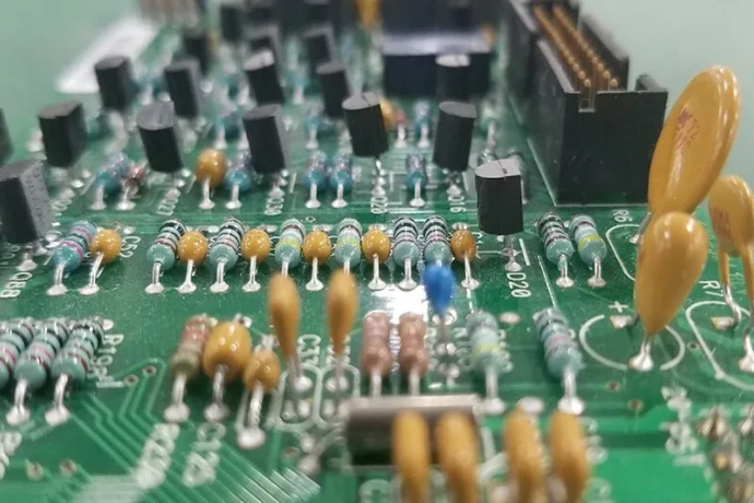
In the wave of AI and high-performance computing (HPC), 2.5D/3D packaging technologies such as CoWoS and EMIB—together with HBM3e high-bandwidth memory—define extreme density and speed at the chip-interconnect level. Yet when we shift our view from micron-scale silicon to system-level interconnects, a “traditional” but critical technology—THT/through-hole soldering—still plays an irreplaceable role. Not only has it not been eliminated by technology evolution; in high-power, high-reliability products such as AI servers, accelerator cards, and switches, it has become a cornerstone for stable operation. From the perspective of an AI packaging and interconnect engineer, this article examines the challenges and solutions for THT/through-hole soldering in modern AI hardware, and how it works together with advanced SMT assembly to deliver robust, efficient system-level interconnects.
For many ultra-miniaturized designs, surface-mount technology (SMT) appears to be the only option. But in AI GPU modules with power budgets reaching kilowatts, the mechanical strength and current-carrying capability required by power connectors, bulk capacitors, and reinforcement hardware are hard for SMT joints to match. That is exactly where THT/through-hole soldering shows its value. Leading manufacturers such as Highleap PCB Factory (HILPCB) understand that a successful AI hardware product requires not only cutting-edge IC substrate capability, but also the ability to integrate these advanced modules reliably into the final system—which depends on deep know-how and tight control of THT processes. Understanding how HILPCB helps optimize your AI interconnect/substrate design is a key step toward success.
Why THT/through-hole soldering is still indispensable in advanced AI systems
Although SMT assembly dominates modern electronics manufacturing thanks to high density and automation, the strategic value of THT/through-hole soldering is increasingly prominent in AI hardware. Its irreplaceability comes from several core advantages that directly address AI systems’ extreme physical and electrical constraints.
First, unmatched mechanical strength. AI accelerator cards and server motherboards are often large and heavy, and must endure transportation, installation, and long-term vibration and mechanical stress. Components such as PCIe slots, high-voltage power input terminals, and heavy heatsink brackets become weak points if connected by SMT alone. With THT, the leads pass through the PCB and are soldered on the opposite side; the solder joint leverages the full board thickness as a structural anchor, providing far higher tensile, shear, and torque resistance than SMT. This robust connection ensures long-term reliability in harsh physical environments.
Second, superior current-carrying and heat-dissipation performance. Peak currents in AI GPU modules can reach hundreds or even thousands of amperes. THT connectors and power terminals typically have thicker leads and larger soldered area, allowing safe transmission of very high current with lower resistance and temperature rise. The leads and large solder fillets also form effective thermal paths, conducting heat into internal Heavy Copper PCB layers or ground planes to support thermal management. For high-power passive components such as bulk electrolytic capacitors, THT packages are often the preferred choice for both heat removal and stable electrical connection.
Finally, design flexibility for certain components. Some special-form-factor or functional parts—transformers, fiber-optic transceiver modules, and custom interfaces—are available only in THT packages. On complex AI system boards, mixing THT and SMT is the norm. A comprehensive Turnkey PCBA service must master both processes to manufacture complex products. THT/through-hole soldering is not “outdated”; it coexists with cutting-edge tech in the AI era as a key pillar for building reliable, high-power hardware systems.
THT’s impact on AI substrate power distribution networks (PDN)
The power distribution network (PDN) is the lifeline of AI systems. Its performance determines whether AI silicon can receive stable, clean power under rapidly changing loads. THT/through-hole soldering plays a crucial role in building high-performance PDNs, affecting the entire path from power input to on-die power delivery.
AI chips are characterized by high average power and extreme transient current (di/dt). To handle this, PDN designs deploy hierarchical decoupling across frequency bands. Bulk electrolytic or polymer capacitors near the power entry and high-current paths are almost always THT packages. These “capacitor banks” are the PDN’s energy reservoir. THT soldering provides the mechanical retention needed to keep these large components secure under vibration. More importantly, THT leads can connect directly to multiple internal power and ground planes; with parallel via arrays, the effective series inductance (ESL) and resistance (ESR) are significantly reduced. This low-impedance connection is key for efficient energy delivery and suppressing voltage droop.
In addition, THT connectors are the gateway for external power to enter the AI board. Whether ATX power interfaces or high-power blind-mate connectors on server backplanes, they rely on THT joints to carry hundreds of amperes. Designing these regions requires careful optimization of via placement, diameter, and count to distribute current evenly and avoid local hotspots. When handling HDI PCB and similar advanced boards, HILPCB uses coupled electro-thermal simulation to predict joint temperature rise and current density—guiding stack-up and copper-pour design to ensure long-term PDN reliability.
Finally, THT vias themselves are critical vertical interconnect elements within the PDN. On AI motherboards with dozens of layers, THT vias are the most reliable way to connect surface power routing to deep internal power planes. With tightly controlled drilling and plating, manufacturers can build low-resistance, high-reliability power conduits that keep the system stable.
Key differences between THT vs. SMT in AI hardware
| Attribute | THT/through-hole soldering | SMT Assembly |
|---|---|---|
| Mechanical strength | Very high: leads penetrate the PCB and form a strong mechanical anchor | Medium: joints are only on the PCB surface and are sensitive to shear and peel |
| Current-carrying capability | Very high: thick leads and large solder area | Limited: constrained by pad size and package type |
| Thermal performance | Good: leads act as thermal paths into internal layers | Moderate: mainly depends on pads and surface copper |
| Assembly density | Lower: components consume both-side space and require drilling | Very high: double-sided placement without drilling |
| Typical components | Connectors, bulk capacitors, transformers, power devices | ICs, resistors/capacitors, small passives, BGA/LGA |
| Automation level | Medium: often wave/Selective wave soldering or manual soldering | High: fully compatible with high-speed placement and reflow |
Managing thermal challenges of THT components: from PCB design to system cooling
While THT components excel at carrying high current, they can also become major heat sources and disrupt airflow, so thermal planning must start early. Thermal design in AI systems is a complex multi-physics problem, and THT components are an important part of it.
First, high-current THT connectors and power inductors are major heat generators. Their heat must be removed effectively to prevent temperature overruns that cause material aging, resistance increase, or even safety hazards. A strong strategy is to use the PCB itself as a heat spreader: design large copper areas around THT components and connect them to internal ground/power planes via dense thermal vias (Thermal Vias), forming an efficient 3D heat network. Internal planes act like fins, distributing heat across the board, where chassis fans or liquid cooling can remove it.
Second, THT components’ physical size and height can affect airflow. In air-cooled servers, airflow passes through CPU/GPU heatsinks and memory modules. Tall THT capacitors or connectors placed poorly can create “airflow shadow zones,” degrading downstream cooling. PCB layout engineers must collaborate with thermal engineers and use CFD simulation to optimize placement and orientation—keeping airflow smooth and avoiding dead zones.
In extreme cases, additional protection and thermal enhancement are required. For automotive AI compute units or industrial edge devices, vibration and moisture threaten THT joints. Here, Potting/encapsulation with thermally conductive epoxy or silicone can fully cover the THT region, providing strong mechanical/environmental protection and improving heat spreading into the enclosure or cold plate. This holistic thermal strategy is essential for long-term stability in harsh AI deployments.
High-speed signal integrity: parasitics of THT vias and optimization strategies
When THT is used for high-speed signal paths—such as connectors between backplanes and daughter cards—its signal integrity (SI) challenges become apparent. A THT via is no longer a simple conductor at high frequency; it behaves like a complex R-L-C network. Parasitic capacitance and inductance introduce impedance discontinuity, reflection, crosstalk, and mode conversion, potentially causing data errors.
The primary SI issue is the via “stub.” When a signal transitions through a via from one layer to another, the unused portion forms an unterminated transmission-line branch. At high speed, the stub can resonate at quarter-wavelength, creating deep notches in S-parameter insertion loss. For PCIe 5.0/6.0 and beyond, this effect can be fatal.
The most effective mitigation is Back-drilling (Back-drilling): after PCB fabrication, a larger drill removes the unused via barrel from the stub side, leaving only the necessary section. This requires extremely tight depth control. As an experienced PCB/substrate manufacturer, HILPCB provides precision backdrilling to minimize stub length and significantly improve channel performance.
Beyond backdrilling, optimizing the via design itself is critical, including:
- Optimize anti-pad (Anti-pad): increasing the clearance in ground/power planes around the via reduces parasitic capacitance and raises via impedance closer to the trace target (typically 50Ω single-ended or 100Ω differential).
- Add ground vias: strategically place one or more ground vias around the signal via and connect them to the reference ground plane. This provides a low-inductance return path and reduces ground bounce and crosstalk.
- Avoid right-angle routing: use smooth arcs or 45° angles when entering/exiting via pads to reduce abrupt impedance changes.
With advanced 3D EM simulation, engineers can model THT via behavior precisely and optimize it in the design stage—ensuring that THT/through-hole soldering can meet strict SI requirements even in the most demanding AI interconnect scenarios.
HILPCB through-hole soldering capability matrix
| Manufacturing parameter | Standard capability | Advanced capability |
|---|---|---|
| Max PCB layer count | 32 layers | 56 layers |
| Max board thickness | 6.0mm | 12.0mm |
| Min mechanical drill size | 0.20mm | 0.15mm |
| Max aspect ratio (Aspect Ratio) | 12:1 | 18:1 |
| Hole position accuracy | ±0.075mm | ±0.05mm |
| Backdrill depth control accuracy | ±0.10mm | ±0.05mm |
| Supported copper thickness | 0.5oz - 6oz | Up to 12oz (heavy copper) |
Selective wave soldering: precision soldering for mixed-technology AI boards
Modern AI boards are typical mixed-technology PCBs: dense SMT components such as BGA and QFN coexist with critical THT connectors and capacitors. After SMT assembly reflow, soldering the remaining THT parts efficiently and reliably becomes a key challenge. Conventional wave soldering immerses the entire PCB underside in molten solder, exposing already-assembled SMT components (especially those on the bottom side) to thermal shock and risking drop-off or damage.
Selective wave soldering is an ideal solution. It uses one or more precisely positioned micro solder nozzles to solder only the targeted THT joints while leaving the rest of the board unaffected. The process is highly automated (CNC-controlled) and can tailor parameters per joint, such as preheat time, solder temperature, nozzle height, and contact time.
In AI hardware manufacturing, the benefits are clear:
- Protect sensitive components: avoids secondary heating of expensive AI silicon, memory modules, and other SMT parts, maximizing yield and reliability.
- Improve solder quality: compared to manual soldering, machine-controlled consistency produces full, uniform joints and reduces human-caused defects.
- Increase design flexibility: controlled solder areas allow denser SMT placement near THT components without solder-interference risk, improving integration density.
- Repeatability: once a program is qualified, it can be replicated precisely across production lots, stabilizing quality.
HILPCB’s advanced assembly lines are equipped with high-precision selective wave systems and strict SPC, ensuring each THT joint meets IPC-A-610 Class 3 requirements for AI/server-grade reliability.
From design to delivery: how Turnkey PCBA simplifies THT integration
For AI hardware companies, managing a complex supply chain is a major challenge. They must source separate PCB fabs, component suppliers, SMT houses, and THT assembly vendors, and coordinate workflows—any delay or quality issue can jeopardize the entire project. Turnkey PCBA consolidates this into a single interface.
A full Turnkey PCBA provider such as HILPCB integrates the entire manufacturing flow. Customers deliver design files (Gerber, BOM) and test requirements and receive fully functional PCBA. When integrating THT/through-hole soldering, the benefits are especially strong:
- Front-end design optimization (DFM/DFA): engineers review not only PCB manufacturability (DFM) but also assembly feasibility (DFA). They focus on THT placement, land design, hole spacing, and safe distances to SMT parts—preventing downstream issues.
- Seamless process handoff: PCB fabrication, SMT assembly, and THT soldering are completed within one factory or under one QA system. This enables end-to-end optimization from materials and surface finish selection (e.g., ENIG vs HASL) to solder-process parameters.
- Unified quality control: consistent standards and inspection across the chain, from bare-board electrical testing to SMT AOI/X-Ray and THT visual checks. Final electrical validation is performed via Flying probe test, ICT, and/or FCT to ensure every net is correct.
- Simplified supply-chain management: one supplier means less communication overhead and logistics complexity, saving time and allowing R&D teams to focus on core architecture and algorithms.
By choosing a reliable Turnkey PCBA partner, companies can ensure that complex AI boards—both dense SMT regions and critical THT regions—are manufactured efficiently and to high quality, accelerating time to market.
🏢 HILPCB end-to-end Turnkey PCBA workflow
From engineering review to precision final testing—an efficient, transparent, high-reliability manufacturing solution.
Deep review of design data to improve manufacturability and mitigate risks before build.
A strong supply chain ensures authentic parts, controlled lead times, and full traceability.
Supports HDI, thick copper, and high-frequency builds with strict electrical/flatness control.
Automated high-precision placement plus selective wave for perfect small + heavy components.
Integrates SPI/AOI/X-Ray and flying-probe/functional testing to support zero-defect delivery.
Ensuring long-term reliability: testing and protection for THT joints
THT joint quality directly affects long-term stability of the entire AI system. A seemingly minor solder defect can rapidly degrade under high current or vibration, leading to intermittent faults or catastrophic failure. Therefore, rigorous testing and effective protection of THT joints are essential steps in manufacturing.
Testing and inspection are the first line of defense:
- Visual inspection and AOI: per IPC-A-610, verify solder fill (typically ≥75%), good wetting, and no pinholes, cracks, or cold joints. AOI supports high-throughput screening.
- X-Ray inspection: for dense leads or joints hidden by component bodies, 2D/3D X-Ray is the only effective non-destructive method. It shows hole fill and reveals internal bubbles/voids.
- Electrical test: Flying probe test is flexible and efficient for prototypes and small batches. Probes move from CAD data to check opens, shorts, and component parameters. For volume production, ICT and/or FCT are commonly used to validate electrical performance.
After passing tests, additional protection may be required depending on the operating environment:
- Conformal coating: a thin polymer layer protects against moisture, salt fog, and dust—especially important for edge AI deployed outside controlled data centers.
- Potting/encapsulation: for extreme shock, vibration, or chemical exposure (e.g., automotive compute platforms), Potting/encapsulation provides the highest level of physical protection. Thermally conductive potting also improves heat dissipation, further increasing reliability.
With a complete workflow from inspection to protection, every THT/through-hole soldering joint can remain rock-solid and support long-term AI system stability.
Future-facing THT: evolving for next-generation AI hardware
As AI silicon power and data rates continue to climb, requirements for system-level interconnects rise as well. THT technology is not standing still; it is evolving through innovation in materials, processes, and form factors to meet next-generation AI needs.
One important direction is press-fit technology (Press-fit Technology). Press-fit connectors use specially shaped compliant pins; when pressed into plated through-holes, the pin elastically deforms and creates high normal force against the barrel, forming a gas-tight cold-weld connection. This solderless approach avoids high temperature, is friendly to heat-sensitive parts, and offers high reliability and serviceability. In modular AI servers where modules are frequently inserted or upgraded, press-fit is becoming increasingly popular.
On the materials side, new high-conductivity, high-reliability solder alloys are being developed to handle higher current and temperature. PCB materials paired with THT components are also upgrading—using higher Tg and lower CTE laminates to reduce solder-joint stress under severe thermal cycling.
In addition, THT component form factors are evolving: more hybrid connectors integrate both power and signal, and THT connectors optimized for high-speed differential pairs are designed with careful internal structures for better impedance control.
Future AI systems will be electro-optically integrated. Fiber connectors and optical engines still require high-precision alignment and long-term mechanical stability, making THT one of the preferred integration methods.
In short, THT/through-hole soldering and related techniques are evolving in step with AI hardware—driving innovation to meet the extreme demands of power, speed, and reliability.
Conclusion: THT soldering as a key process for robust AI systems
While it is easy to be amazed by billions of transistors inside AI chips, we must not overlook the physical foundation that allows these compute engines to operate reliably. THT/through-hole soldering, with inherent advantages in mechanical strength, power delivery, and thermal management, remains a critical building block in today’s and tomorrow’s AI hardware ecosystem. Together with advanced SMT assembly, it forms the manufacturing backbone of complex AI PCBs.
From PDN optimization and SI mitigation to precision production with Selective wave soldering, and supply-chain simplification via Turnkey PCBA, mastering the details of THT/through-hole soldering is a necessary step toward successful AI products. Partners like HILPCB, providing one-stop solutions from PCB fabrication to through-hole assembly (through-hole assembly), create value by deeply understanding and controlling these “traditional but essential” processes—ensuring innovative designs become reliable, high-performance physical products. Ultimately, it is these strong solder joints that support the AI era’s computing infrastructure.
Contact HILPCB to start your AI substrate/interconnect project—let our manufacturing expertise empower your innovation.