
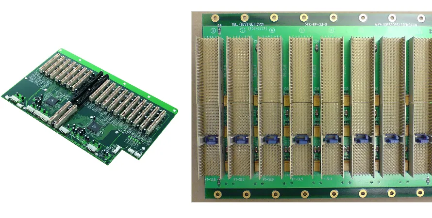
With exponential growth in AI and ML compute demand, AI server hardware design faces unprecedented challenges. As the core hub connecting compute, storage, and networking subsystems, server backplane PCB design and manufacturing directly determine overall system performance and stability. Although SMT has become mainstream, for connectors that must carry high current, withstand many mating cycles, and survive severe mechanical stress, THT/through-hole soldering is not “obsolete”—it remains indispensable in AI server backplanes thanks to its exceptional reliability.
However, at PCIe 5.0/6.0 and beyond, traditional THT becomes a major SI bottleneck. Mastering THT/through-hole soldering challenges—balancing mechanical strength, PI, and high-speed SI—is a problem every AI hardware engineer and PCB manufacturer must solve. It demands not only excellent process capability but end-to-end optimization from materials and stackup to soldering processes. As an industry-leading PCB solution provider, Highleap PCB Factory (HILPCB) delivers advanced manufacturing and assembly services aligned with next-generation AI server needs.
Why THT/through-hole soldering is still indispensable in AI server backplanes
SMT is strong in density and automation, but in AI server backplanes, THT/through-hole soldering provides unique physical advantages that SMT can’t match—making it the preferred technology for critical connector mounting.
Unmatched mechanical strength and durability: backplane connectors (e.g., Orthogonal Midplane Connectors, OCP NIC 3.0 connectors) are large, pin-dense, and must tolerate frequent insertion/removal stress. THT pins pass through the PCB and are fully wetted by solder, creating a bond far stronger than SMT pad adhesion. This robust attachment is key to long-term AI server motherboard PCB reliability, reducing failures from vibration or shock.
Excellent high-current capability: AI accelerator cards (GPU, TPU) can exceed 1000W and require hundreds of amps distributed through the backplane. THT pins and PTH barrels provide much larger cross-section than SMT pads, carrying large current with lower resistance and less heating. This is critical for a stable PDN, reducing IR Drop and delivering clean power to core devices.
Simplified thermal paths: THT pins also provide a helpful heat-conduction path, transferring connector heat into internal PWR/GND layers, where large copper areas act as built-in heat spreaders.
So in performance-first AI server designs, THT/through-hole soldering is not a legacy choice—it is a strategic choice for high-reliability, high-power interconnect.
High-speed SI: SI challenges of THT vias and optimization
In the 56/112 Gbps PAM4 era, the THT connector via itself becomes a major SI challenge. Unoptimized vias can severely degrade high-speed quality.
- Via stub effect: in multilayer PCBs, signals often traverse only some layers. The unused via portion forms a “stub” that resonates like an antenna, causing strong reflections and Insertion Loss and potentially closing the eye.
- Impedance discontinuity: the via barrel geometry changes the line shape, creating an impedance step that increases Return Loss and introduces Jitter.
- Via-to-via crosstalk: in dense connector fields, adjacent THT vias couple electromagnetically, leaking energy between channels—especially harmful for differential pairs.
To overcome these issues, precise AI server motherboard PCB routing and manufacturing strategies are required. The most critical technique is Back-drilling/Controlled Depth Drilling, which removes unused stub length from the opposite side and minimizes resonance. A successful back-drill process typically controls the remaining stub to within 10mil (~254μm), requiring excellent depth-control accuracy. Optimizing Anti-pad sizing, tuning nearby reference planes, and adding ground-via shielding are also effective for impedance matching and crosstalk suppression.
SI performance comparison before/after THT via optimization (simulation @ 28 GHz)
| Metric | Standard THT via (unoptimized) | Optimized THT via (with back-drill) | Improvement |
|---|---|---|---|
| Insertion Loss | -4.5 dB (severe attenuation) | -1.2 dB (significantly improved) | Improved 73% |
| Return Loss | < -10 dB (strong reflection) | < -18 dB (good match) | Reflection reduced > 8 dB |
| Stub resonance point | ~15 GHz (limits bandwidth) | > 40 GHz (moved out of band) | Resonance shifted > 160% |
How backplane stackup affects THT performance
A well-designed AI server motherboard PCB stackup is the foundation for high-performance THT/through-hole soldering. Stackup defines electrical properties and directly impacts manufacturability and cost.
First, material selection is critical. To support high-speed links, AI backplanes commonly use Ultra-Low Loss materials such as Megtron 6/7 and Tachyon 100G. With very low Dk and Df, these materials reduce attenuation. Using flat copper foils (HVLP) and Spread Glass helps minimize Fiber Weave Effect and keeps differential impedance more uniform.
Second, layer count and thickness are key. AI backplanes are often 20–40 layers and can exceed 6mm thickness. Such thick PCBs challenge THT, especially drilling Aspect Ratio. High aspect-ratio holes (18:1 and above) require extremely uniform copper plating; any thin plating can cause opens or reliability issues.
Finally, continuous reference planes are essential for a clean return path. In the connector region, every signal via needs a nearby, solid ground or power reference plane. Any splits/voids break the return path and increase EMI and crosstalk. HILPCB engineers have deep High-Speed PCB experience and can help optimize stackups for best electrical performance.
Power integrity (PI): high-current challenges of THT connectors
Another core task of AI backplanes is delivering stable power to hundreds or thousands of processor cores. THT connectors are key to this job; their PI design directly impacts system stability.
The main challenge is managing huge current and the resulting IR Drop. For example, a GPU power connector may carry >500A at 12V or 48V. Even with very low pin resistance, such current can create significant voltage drop across PCB traces, vias, and pins. Excessive drop can cause GPU undervoltage, throttling, or crashes.
Solutions include:
- Heavy copper / ultra-heavy copper: use 3oz or thicker copper on power/ground planes to reduce plane resistance. HILPCB provides Heavy Copper PCB fabrication for high-current needs.
- Optimize power paths: keep power routing wide and short, and allocate multiple THT pins/vias for high-current nets to parallelize current and reduce resistance.
- Precise decoupling placement: place sufficient decoupling capacitors near THT power connectors to supply transient current and suppress rail noise.
A strong PDN is the cornerstone for AI server motherboard PCB mass production yield and long-term stability.
Key points for THT power integrity design
- ✅ Minimize loop inductance: keep PWR and GND pins adjacent and shorten return paths.
- ✅ Control IR Drop: calculate drop with PI simulation tools, then optimize using heavy copper or more plane layers.
- ✅ Strategic decoupling: deploy a multi-level decoupling network (high/mid/low frequency) between connector and load (e.g., VRM).
- ✅ Electro-thermal co-design: evaluate Joule heating on high-current paths, keep temperature within safe limits, and avoid impacting **AI server motherboard PCB reliability**.
Thermal management and reliability strategy for THT soldering
Soldering is the final—and most critical—step of THT/through-hole soldering. For thick, high-thermal-mass AI backplanes, traditional Wave Soldering is challenging: the PCB absorbs large heat, leaving insufficient temperature at the soldering region and causing cold joints and opens.
Modern THT processes therefore increasingly use:
- Selective Soldering: a mini solder nozzle heats/solders only the required THT pin area. It controls heat input precisely, avoids thermal shock to nearby SMT, and is ideal for mixed-technology (SMT+THT) boards.
- Pin-in-Paste / Intrusive Reflow: print solder paste into THT holes, insert pins, and run the full board through reflow. Paste melts and fills the barrel to form a reliable joint. This is SMT-compatible, simplifies flow, and is especially suitable for AI server motherboard PCB quick turn.
Long-term joint reliability is also critical. IPC-A-610 specifies Barrel Fill requirements for THT joints, typically 75%+. To ensure no voids or cracks inside, X-Ray is needed for non-destructive inspection.
DFM: ensure manufacturability and yield for THT backplanes
A theoretically perfect backplane PCB can still suffer low yield, high cost, or even be unbuildable if DFM is ignored. For complex THT backplanes, DFM is especially important.
- Aspect Ratio: board thickness divided by minimum drill diameter. Too high an aspect ratio makes plating chemistry hard to reach the hole center, thinning copper there. The fab must declare capability; designers must stay within it.
- Annular Ring: the copper ring around a drilled hole. Ensure sufficient width so drill-position tolerances don’t break the ring; IPC defines class requirements.
- Spacing and tolerances: hole-to-copper, hole-to-hole spacing, and back-drill depth tolerance. These directly affect electrical performance and yield.
To help customers avoid these risks, HILPCB provides free DFM analysis. Our engineers review files before production, identify manufacturability challenges, and propose optimizations—building a solid base for AI server motherboard PCB mass production.
HILPCB high-complexity backplane manufacturing capability
| Process parameter | HILPCB capability |
|---|---|
| Max layer count | 64 layers |
| Max PCB thickness | 10.0 mm |
| Max drill aspect ratio | 20:1 |
| Back-drill depth control | ± 50 µm |
| Impedance control tolerance | ± 5% |
| Supported materials | Megtron 6/7, Rogers, Tachyon 100G, etc. |
How HILPCB delivers high-reliability THT/through-hole soldering
HILPCB understands the extreme reliability requirements of AI backplanes. By combining advanced equipment, strict process control, and deep engineering expertise, we ensure every THT/through-hole soldering operation meets the highest standard.
- Advanced fabrication and assembly equipment: we invest in high-precision mechanical and laser drilling, advanced plating lines, and automated equipment for selective soldering and intrusive reflow—ensuring consistency from drilling and plating to soldering.
- Strict quality control: AOI for inner-layer circuitry and X-Ray for multilayer registration and THT barrel fill. All products undergo electrical and reliability tests (e.g., thermal shock), ensuring every delivered backplane PCB is rock-solid.
- One-stop solution: from optimizing AI server motherboard PCB stackup and AI server motherboard PCB routing, to quick-turn prototypes and volume production, to high-quality through-hole assembly, HILPCB provides seamless end-to-end delivery. This integration improves quality and shortens time-to-market, supporting AI server motherboard PCB quick turn.
FAQ
Why is THT/through-hole soldering still critical for AI server backplanes?
AI server backplanes still rely on large connectors and mechanically stressed interfaces that must carry high current and survive long service life. THT/through-hole soldering remains the most robust way to anchor these components while preserving electrical and mechanical reliability.
What design risks most often hurt THT backplane manufacturability?
The biggest risks usually come from excessive drill aspect ratio, insufficient annular ring, poor hole spacing, and unmanaged back-drill tolerances. These issues can reduce plating quality, weaken solder joints, and create yield loss before assembly is even optimized.
How should teams verify THT solder quality on high-complexity backplanes?
Teams should combine IPC-A-610 barrel-fill criteria with X-Ray inspection, electrical testing, and reliability screening such as thermal shock. This layered validation catches both visible solder defects and hidden structural problems inside the plated barrel or joint.
Why does choosing an experienced manufacturing partner matter so much here?
For AI backplanes, fabrication, soldering, DFM review, and reliability validation are tightly linked. An experienced partner can align stackup, drilling, plating, solder process, and inspection from the start, which lowers build risk and improves mass-production stability.
Conclusion
In modern AI server backplanes, THT/through-hole soldering remains essential. It is no longer “simple insertion soldering”, but a complex engineering discipline combining high-speed SI, PI, thermal management, and precision manufacturing. Successfully executing it requires close collaboration between design engineers and experienced PCB manufacturers like HILPCB.
With advanced back-drilling, careful stackup design, robust PDN, and controllable soldering processes, we can combine THT connectors’ reliability advantages with high-speed transmission requirements. If you are developing next-gen AI servers, switches, or HPC systems and need a partner that deeply understands and solves THT/through-hole soldering challenges, HILPCB is the right choice.