
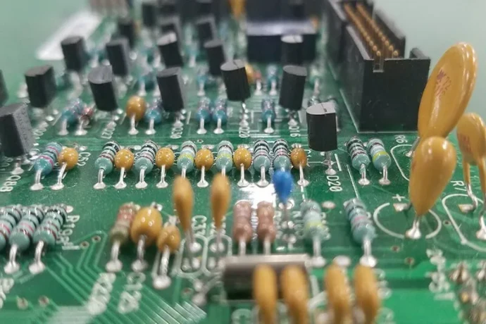
THT soldering is the process of inserting component leads into plated through-holes and forming soldered electrical and mechanical joints. In a high-speed PCB, the soldering process and the through-hole interconnect geometry are related but different engineering problems: solder quality determines joint integrity, while the pin, barrel, pads, antipads, return vias, breakout routing, and unused stub determine much of the signal-integrity behavior.
This guide helps hardware, signal-integrity, manufacturing, and sourcing teams choose a termination process, define a connector launch, and release evidence that can be checked instead of relying on a generic instruction such as “build to IPC.”
Key Takeaways
- Through-hole does not automatically mean soldered. A compliant press-fit connection is solderless and needs its own hole, tooling, force, and inspection controls.
- Data rate alone does not decide whether a transition is electrically critical. Edge rate, channel bandwidth, topology, loss budget, return path, and receiver margin matter.
- A connector vendor's S-parameter model may stop at the connector pins and exclude the application-specific PCB breakout. Model reference planes must therefore be documented.
- Backdrilling is a controlled fabrication operation, not a note added after layout. Release data should define the target holes, drill file, depth or layer range, residual-stub requirement, and clearances.
- Wave, selective, hand or robotic soldering, pin-in-paste reflow, and compliant press-fit solve different production problems. None is the universal best route.
- Inspection should be selected by defect visibility and risk. Visual inspection is central for accessible THT joints; X-ray can add internal information but is not an unlimited or self-interpreting acceptance method.
Contents
- What Does THT Mean in a High-Speed PCB?
- When Does Through-Hole Hardware Belong in the Design?
- How Does a Through-Hole Transition Affect Signal Integrity?
- What Evidence Defines a High-Speed Connector Launch?
- Which Termination Process Should You Choose?
- How Should Mixed SMT and THT Assembly Be Planned?
- What Should DFM, DFA, and DFT Review Cover?
- How Should THT Joints Be Inspected and Tested?
- What Common Failures and Changes Require Requalification?
- What Should Be Included in a THT High-Speed RFQ?
What Does THT Mean in a High-Speed PCB?
Three structures are often mixed together under the label “THT,” yet they create different design and acceptance responsibilities.
- Plated through-hole interconnect: the PCB barrel, pads, antipads, layer connections, and any unused barrel below or above the signal transition.
- Soldered through-hole termination: a lead or pin is inserted and soldered by wave, selective, hand, robotic, or intrusive-reflow processing.
- Compliant press-fit termination: a compliant pin is mechanically inserted into a qualified plated hole to create a solderless electrical contact.
The first structure exists in both soldered and press-fit connector systems. It is the main bridge between PCB fabrication and signal-integrity design. The second adds flux, preheat, solder access, thermal balance, joint acceptance, and cleaning decisions. The third removes solder from the termination but adds press tooling, board support, insertion-force monitoring, plated-hole compatibility, and connector-specific application requirements.
This distinction prevents two expensive misunderstandings. First, changing from soldered pins to press-fit pins is not merely an assembly-process substitution; the connector, finished-hole system, qualification evidence, and sometimes launch geometry change. Second, a cosmetically acceptable solder joint does not prove that the signal transition meets its insertion-loss, return-loss, crosstalk, or skew budget.
When Does Through-Hole Hardware Belong in the Design?
Through-hole hardware remains useful where the component form factor, interface standard, retention strategy, or service environment requires it. Common examples include large board-to-board and cable connectors, terminal blocks, transformers, relays, switches, tall electrolytic capacitors, and mechanically loaded controls. High-layer-count backplane PCB designs also frequently use through-hole or press-fit connector fields.
Mechanical strength should be evaluated at the assembly level, not assumed from lead style. A lead passing through the board can provide useful retention, but durability still depends on connector housing support, fasteners, board flex, insertion and extraction loads, hole and pad integrity, solder geometry, enclosure constraints, vibration spectrum, and service cycles. A heavily loaded connector may need chassis support even when every pin is through-hole.
The same caution applies to current and heat. Some leaded parts are designed for substantial current or thermal transfer, but a THT lead is not automatically a high-current bus or a heat sink. The component data sheet, pin material, contact resistance, copper connection, plated-hole construction, temperature rise, cooling path, and system derating determine the usable result. Thermal relief geometry must balance solderability against electrical and thermal requirements; applying it by habit can either starve a joint of heat or add unwanted impedance.
A practical architecture decision therefore starts with four questions:
- Does the interface or component actually require a through-hole package?
- What loads must be reacted by the pins, PCB, connector hardware, and enclosure?
- Is the pin part of a critical signal, power, return, shield, or low-speed control path?
- Which termination route can be manufactured, inspected, repaired, and repeated at the intended volume?
How Does a Through-Hole Transition Affect Signal Integrity?
A high-speed transition becomes important when its electrical length and discontinuity consume meaningful channel margin. The relevant stimulus is the signal edge and its frequency content, not only the nominal clock or bit rate. A low-clock control signal with a fast driver can be more sensitive to a poor transition than its frequency label suggests.
The connector launch should be treated as a three-dimensional electromagnetic structure. Current travels through the signal pin and via while return current must cross the same region through reference planes, ground pins, stitching vias, or other intended return conductors. Pad fields, antipad openings, plane cavities, routing layers, and nearby pins all interact.
| Risk | Physical cause | What may appear in the channel | Useful controls |
|---|---|---|---|
| Unused via stub | Barrel continues beyond the signal layer | Resonance, return-loss degradation, insertion-loss notch, eye closure | Shorter transition, stackup change, blind structure where appropriate, controlled backdrill |
| Local impedance discontinuity | Pin, barrel, pad, antipad, and plane geometry differ from the trace | Reflection and reduced voltage margin | Field-solved launch, padstack and antipad tuning, correlation by TDR or VNA |
| Return-path discontinuity | Reference-plane change or insufficient nearby return connection | Common-mode conversion, radiation, crosstalk | Intentional return vias or ground pins, continuous reference strategy, cavity control |
| Differential asymmetry | Unequal pin fields, breakout routes, stubs, or return geometry | Intra-pair skew and mode conversion | Pair-symmetric launch, matched layer transitions, model both conductors and returns |
| Via-field crosstalk | Coupling among signal pins and through-hole barrels | Near-end or far-end coupling and lane-to-lane noise | Pin assignment, spacing, ground pattern, antipad/cavity design, multiport model |
| Model-boundary error | Connector model omits breakout or uses unclear reference planes | Simulation looks better or worse than the manufactured channel | Document ports, include the missing PCB launch, cascade only compatible models |
Backdrilling removes an unused barrel section with a larger controlled-depth drill. It can reduce a harmful stub, but the production release must do more than state “backdrill high-speed vias.” It should identify the holes, supply the dedicated NC drill data, define the drilled side and first/last layer or depth intent, state the allowed residual stub, and account for drill diameter and clearance to pads, planes, traces, and nearby component features. Fabricator capability and registration tolerances determine the final manufacturable values.
Stub resonance should not be accepted using one universal quarter-wave shortcut. Physical length is important, but pad geometry, fringe capacitance, dielectric behavior, and the complete transition alter the result. For a margin-sensitive link, use a suitable 3D model and correlate the assumptions with measurement.
What Evidence Defines a High-Speed Connector Launch?
The strongest release package makes every simulation boundary traceable to the physical design. Connector vendors commonly provide S-parameters or electromagnetic models, but those files do not always include the customer's stackup, pad field, escape routing, or nearby return-via pattern. The engineering team must confirm what is inside the model before cascading it with PCB traces.
Use the following evidence package for each electrically critical connector family:
| Evidence item | Minimum question it must answer | Why it matters |
|---|---|---|
| Connector identity | What exact part number, revision, pin map, and termination style is modeled? | Similar connector variants may not share the same launch or channel behavior. |
| Stackup | What finished thicknesses, copper layers, reference planes, and dielectric assumptions apply? | Propagation, impedance, loss, and via geometry depend on the released construction. |
| Padstack | What drill, finished hole, pad, nonfunctional pad, and antipad geometry is used by layer? | The vertical discontinuity cannot be reproduced without it. |
| Signal and return topology | Which pins/vias carry signals and which provide the high-frequency return path? | Return geometry is part of the transmission line. |
| Layer transition | Where does each signal enter and exit, and what unused barrel remains? | Stub length and asymmetry depend on the actual routing layer. |
| Backdrill definition | From which side, to what layer/depth, with what residual-stub and clearance intent? | This connects SI intent to fabricator data and inspection. |
| Model reference planes | Where are the S-parameter ports, and does the model include PCB breakout? | Undefined or overlapping model boundaries invalidate channel cascades. |
| Application launch model | How are the real breakout, return vias, planes, and nearby lanes represented? | A connector-only model cannot qualify an omitted PCB launch. |
| Correlation plan | Will a coupon or product be checked by TDR, VNA, eye/BER test, or another agreed method? | Measurement establishes whether the released model represents production hardware. |
| Acceptance record | Which plots, limits, revisions, and lot/build identifiers are retained? | A screenshot without conditions or revision identity is not durable evidence. |
S-parameters describe insertion loss, return loss, and coupling as a function of frequency and can support full-channel analysis when ports and reference impedances are compatible. They do not, by themselves, prove protocol compliance, production yield, or environmental reliability. The channel owner must define the system budget and acceptance method.
Which Termination Process Should You Choose?
The termination route should be frozen early enough to influence footprint design, component sourcing, panelization, keepouts, fixtures, inspection, and repair. The following matrix is a decision asset, not a substitute for component-vendor application requirements or assembly trials.
| Termination architecture | Best-fit use | SI model boundary | PCB and assembly controls | Release evidence | Change-control trigger |
|---|---|---|---|---|---|
| Soldered THT with wave soldering | Many accessible bottom-side joints with wave-compatible layout and volume | Connector/pin plus complete PCB launch; solder shape is normally secondary unless the model specifically includes it | Wave direction, pallet need, component and mask clearances, preheat, thermal balance, lead length, flux and cleaning plan | Approved profile/setup, first-article joint inspection, defined workmanship class, electrical test | New connector plating, board thermal mass, pallet, alloy/flux, hole system, or component shadowing |
| Soldered THT with selective soldering | Mixed technology, localized THT joints, or bottom-side SMT that cannot enter a broad solder wave | Same electrical launch boundary; ensure nozzle/keepout changes do not force padstack or return-via changes | Nozzle access, keepout, board support, preheat, dwell and wetting window, adjacent-part temperature exposure | Program revision, thermal/process record as required, joint inspection, test results | Nozzle/program change, new nearby component, copper-balance change, board thickness or finish change |
| Hand or robotic soldering | Prototype, low volume, repair, or geometries poorly suited to wave/selective equipment | Same launch definition; rework must not damage barrel, pad, or adjacent return structures | Tip access, heat input, operator/program control, flux and cleaning, lead stability, rework limit | Work instruction, trained-process record as required, inspection and continuity/function test | Tool, tip, solder/flux, operator qualification method, access, or rework cycle change |
| Pin-in-paste or intrusive reflow | Reflow-compatible THT parts intended to join during the SMT reflow cycle | Connector launch plus the released plated-hole/pad geometry | Component reflow rating, paste-volume calculation, stencil apertures/steps, insertion displacement, support, profile and residue plan | Paste and profile record, first-article fill/wetting evaluation, placement and electrical test | Stencil, paste, component coplanarity, board thickness, hole/lead geometry, or reflow profile change |
| Compliant press-fit | Qualified solderless connector system, commonly used for dense connector fields or thermal-process avoidance | Connector pin plus PCB launch; use the press-fit variant's geometry and model | Connector-specific finished-hole/plating window, board support, press tooling, alignment, insertion-force monitoring, repair limits | Hole data, tool/program revision, force-displacement record when specified, inspection and electrical test | Connector/pin revision, hole finish or plating, board thickness, tool, press program, or repair method change |
Pin-in-paste is not simply “put paste in the hole.” The assembly must deliver enough solder to form the specified joint after paste displacement and volatile loss while avoiding bridging, floating, or contamination. The component must also be approved for the applicable reflow exposure. Stencil design, paste transfer, lead-to-hole fit, board thickness, component seating, and thermal profile work as one system.
Press-fit is likewise not “THT without the soldering step.” The compliant section and plated hole are a qualified contact pair. Substituting a different connector, hole finish, plating construction, press tool, or repair approach can change insertion forces, barrel stress, contact behavior, and signal performance.
How Should Mixed SMT and THT Assembly Be Planned?
A mixed assembly route is usually SMT printing, placement, and reflow followed by insertion and the selected THT operation, but that sequence is not universal. Double-sided SMT, bottom-side wave-compatible components, pin-in-paste connectors, press-fit operations, cleaning restrictions, conformal coating, test access, and mechanical hardware can all change the route.
Wave soldering processes many joints together and can be efficient when the underside layout, component temperature limits, solder-mask design, shadowing, and pallet strategy are compatible. Selective soldering applies flux, preheat, and solder locally and is often advantageous for mixed assemblies, but it needs nozzle access, travel time, stable board support, and a validated program. Selective does not automatically mean lower thermal risk; local dwell and copper heat sinking still require control.
For mechanically large connectors, define when retention hardware is installed and whether it affects solder access, component seating, board flatness, or inspection. For high-speed fields, protect the launch geometry from late assembly-driven edits. Moving a return via to create nozzle clearance, changing an antipad to improve thermal behavior, or enlarging a pad to increase solder access may alter the validated electrical model.
HILPCB's through-hole assembly service can be evaluated as part of a mixed-technology route, but the RFQ should identify the required process rather than assuming every THT footprint can run through the same line setup.
What Should DFM, DFA, and DFT Review Cover?
DFM, DFA, and DFT should converge on one released design. A fabrication review that ignores selective-solder nozzle access is incomplete, just as an assembly edit that changes a high-speed antipad without SI review is incomplete.
PCB fabrication and SI review
- Confirm the stackup, material construction, controlled-impedance structures, and reference planes used by the analysis.
- Check drilled and finished-hole definitions against the selected connector and fabricator process.
- Review pads, antipads, nonfunctional-pad treatment, plane clearances, annular features, and breakout routing.
- Define signal and return-via placement together; do not tune antipads before the topology is stable.
- Release backdrill holes, drill side, depth/layer intent, residual stub, diameter, and clearance data explicitly.
- Include coupons or product measurement structures when correlation is part of acceptance.
Assembly review
- Confirm component body, lead, standoff, seating, polarity, retention, and reflow or soldering compatibility.
- Check wave direction, pallet or nozzle access, keepouts, preheat exposure, thermal mass, and solder drainage.
- Define whether thermal reliefs are electrically and thermally acceptable instead of adding them automatically.
- Review bottom-side SMT components for the selected solder process and fixture strategy.
- Establish flux, residue, cleaning, moisture, masking, coating, and rework constraints from product requirements.
- Protect connector mating surfaces and press-fit zones from contamination and handling damage.
Test review
- Provide accessible test points for rails, grounds, clocks, resets, interfaces, and diagnostic nodes where physical probing is appropriate.
- Define continuity, shorts, in-circuit, functional, boundary-scan, or system-link tests by fault coverage, not by equipment availability alone.
- Boundary-scan/JTAG can detect supported digital interconnect faults, but it cannot prove analog margin, every passive value, connector mating performance, or high-speed channel compliance.
- State fixture interfaces, firmware, loads, limits, data retention, and failure-disposition rules.
- Keep high-speed measurement reference planes and calibration/de-embedding methods consistent with the channel model.
How Should THT Joints Be Inspected and Tested?
The drawing or quality plan should state the applicable standard revision, product class, customer-specific requirements, and which document controls if requirements conflict. J-STD-001 addresses soldered assembly requirements and process/material expectations; IPC-A-610 provides assembly acceptability criteria. They are complementary, and the purchase order should not treat either title as a complete product test specification.
Accessible THT solder joints are commonly evaluated visually for wetting, solder distribution, lead condition, bridging, disturbance, and related workmanship attributes under the invoked acceptance criteria. AOI may improve coverage and consistency where the joint geometry and line-of-sight suit the equipment, but the program needs representative defect validation.
X-ray can reveal internal density patterns and support investigation of barrel fill or obscured structures. It also has limitations: overlapping geometry, board thickness, viewing angle, resolution, and interpretation can hide or mimic defects. X-ray should therefore be specified where it answers a defined risk, with a validated method and acceptance basis, rather than called the “ultimate” inspection for every THT joint.
Electrical and functional evidence addresses different risks:
- Continuity and shorts testing checks basic network connectivity but not necessarily component function or high-speed margin.
- ICT can check accessible nets and components according to fixture and coverage design.
- Boundary-scan/JTAG can exercise supported digital pins and interconnects when the design includes a usable chain and test description.
- Functional test checks behavior under defined stimuli, loads, firmware, and limits; vague “power-on test” language is insufficient.
- TDR or VNA measurement can correlate transition impedance or frequency-domain behavior when the fixture, reference planes, calibration, and de-embedding are defined.
- Protocol, eye, jitter, or BER testing may be needed at system level when link compliance and operating margin are the actual acceptance questions.
No single inspection proves joint workmanship, electrical connectivity, channel performance, and field reliability at once. The control plan should map each known failure mode to the evidence capable of detecting it.
What Common Failures and Changes Require Requalification?
The most costly defects often occur at interfaces between disciplines. A soldering engineer may solve insufficient fill by changing pad or thermal geometry, while the SI model still represents the old launch. An SI engineer may tighten a return-via pattern that blocks the selective-solder nozzle. Change control must therefore cover both electrical and manufacturing boundaries.
| Failure or drift | Likely contributors | Evidence to review before release |
|---|---|---|
| Incomplete or inconsistent solder fill | Lead-to-hole fit, oxidation, thermal mass, preheat, flux activity, access, dwell | Hole/lead data, thermal profile or program, joint inspection, cross-section during process development if justified |
| Bridging or solder icicles | Pad spacing, lead length, solder drainage, conveyor/nozzle parameters, excess paste | Layout and mask review, process setup, visual/AOI evidence, shorts test |
| Barrel, pad, or laminate damage | Excess heat, repeated rework, unsupported press force, unsuitable hole/pin system | Rework history, microscopy, hole/connector specifications, force trace where applicable |
| Connector seating or coplanarity error | Fixture, retention, insertion method, paste buoyancy, warped board | Seating criteria, fixture check, visual/mechanical inspection, mating verification |
| Unexpected return-loss notch | Longer residual stub, padstack change, model-boundary gap, laminate assumption | Fabrication data, backdrill evidence, updated EM model, TDR/VNA correlation |
| Lane crosstalk or skew | Return-via change, asymmetric breakout, pin-map revision, nearby-lane coupling | Multiport model, layout revision, channel simulation, measurement plan |
| Intermittent field contact | Mechanical load, connector support, contamination, press-fit damage, mating wear | Mechanical architecture, connector application requirements, environmental/system qualification |
Requalification depth should be proportional to the affected risk. A silkscreen edit normally does not need a new channel simulation. A change to connector part number, stackup, padstack, antipad, return-via topology, routed layer, backdrill depth, laminate, press-fit hole system, stencil, solder alloy, selective program, or rework method may require targeted review and renewed evidence.
What Drives Cost and Schedule?
THT cost is not determined by joint count alone. Manual insertion, lead preparation, polarity verification, fixtures, selective-solder cycle time, wave pallets, press tooling, inspection access, cleaning, rework, high-speed modeling, coupons, and test fixtures can dominate. A cheap connector substitution may also force a new footprint, launch model, press tool, or qualification build.
Procurement can reduce uncertainty by separating one-time engineering from recurring production cost:
- One-time items: SI model development, coupon design, wave pallet, selective program, press tooling, ICT/FCT fixture, software, and process qualification.
- Per-build items: insertion labor, soldering or pressing cycle time, consumables, inspection, electrical test, cleaning, handling, and data retention.
- Risk items: connector availability, approved alternates, minimum order quantity, long-lead tooling, special laminate, backdrill complexity, and requalification triggered by substitutions.
Early volume assumptions matter. A hand-soldered prototype route may be appropriate for ten boards but give misleading cost, accessibility, and process evidence for a larger release. Conversely, expensive production tooling may not be justified before the connector and launch are stable.
What Should Be Included in a THT High-Speed RFQ?
A complete RFQ allows PCB fabrication, assembly, SI, sourcing, and test teams to quote the same product. Send controlled files rather than relying on screenshots or email-only exceptions.
Design and fabrication files
- Native or exported fabrication data, drill and route files, drawings, netlist, panel constraints, and revision history
- Released stackup with impedance requirements, materials or performance constraints, copper weights, and finish
- Plated-hole, padstack, antipad, nonfunctional-pad, and backdrill definitions
- Controlled-impedance coupon and TDR/VNA requirements, including reporting expectations
- Connector keepouts, mating interface, mechanical support, and critical dimensions
BOM and component data
- BOM with manufacturer part numbers, approved alternates, lifecycle status, and do-not-substitute items
- Connector drawings, application specifications, termination style, pin map, and vendor models
- Lead dimensions, plating, temperature limits, moisture or handling requirements, and press-fit hole requirements where applicable
- Customer-supplied or consigned material identification and traceability expectations
Assembly process requirements
- Intended route: wave, selective, hand/robotic, pin-in-paste, compliant press-fit, or a defined combination
- Solder alloy, flux or cleanliness constraints, conformal-coating and masking requirements, and rework limits
- Product class, workmanship standard and revision, customer-specific acceptance criteria, and first-article expectations
- Required process records, force traces, thermal data, inspection images, or lot traceability
Signal-integrity and test package
- Interface, lane rate, driver edge assumptions, topology, channel budget, and compliance target
- Connector S-parameter source, revision, port map, reference impedance, and documented reference planes
- Application-specific PCB launch model and cascade/de-embedding method
- Test-point and boundary-scan files, test firmware, fixtures, loads, pass/fail limits, and data format
- TDR, VNA, eye, protocol, BER, ICT, FCT, or system-test requirements with sample size and disposition rules
Commercial and program data
- Prototype, pilot, and production quantities; target dates; forecast; and acceptable panel or process assumptions
- Packaging, labeling, serialization, shipping, regulatory, and documentation requirements
- Ownership and maintenance responsibility for pallets, press tools, fixtures, programs, and test software
- Formal change-notification and requalification expectations for connector, material, process, and geometry changes
How Can HILPCB Support a Mixed-Technology Release?
HILPCB can review a released data package across PCB fabrication, high-speed PCB constraints, SMT, THT, sourcing, and test planning. The useful starting point is not a request for a generic “best process,” but the connector identity, stackup, volume, available model, mechanical load, inspection class, and acceptance evidence your system needs.
For a turnkey PCB assembly quotation, ask for assumptions and exclusions to be written into the response. Confirm which termination route is quoted, which fixtures or programs are one-time charges, what model and backdrill data remain customer-owned, what tests are included, and which changes require renewed approval. This makes the quote comparable and prevents a prototype-only process from silently becoming the production baseline.
HILPCB's manufacturing review does not replace connector-vendor application requirements, customer SI ownership, protocol compliance testing, safety evaluation, or end-product environmental qualification. Final performance and regulatory responsibility remain at the product and system level.
Reference Standards and Specifications
Confirm the current revision, contractual precedence, product class, and applicable amendments for the program. Do not infer a numeric acceptance limit from a standard title alone.
- IPC J-STD-001 — IPC
- IPC-A-610 — IPC
- IPC-2221 — IPC
- IPC-2222 — IPC
- IPC-6012 — IPC
- IEC 61191-3 — International Electrotechnical Commission
- Connector manufacturer application specification
- Interface or protocol compliance specification selected by the system owner
Common Questions
Is every through-hole connector soldered?
No. A conventional THT connector may use wave, selective, hand, robotic, or pin-in-paste soldering, while a compliant press-fit connector uses a solderless mechanical contact in a qualified plated hole. The footprint and process must match the exact connector termination style.
Does a higher data rate always make a THT connector unsuitable?
No. Suitability depends on the complete channel, including edge rate, loss budget, connector design, pin assignment, PCB launch, return path, unused stub, crosstalk, receiver margin, and measurement correlation. Data rate alone is not an adequate pass/fail rule.
When is backdrilling needed for a connector launch?
Backdrilling is considered when an unused plated-barrel stub consumes meaningful channel margin. The decision should come from the released geometry and channel analysis, then be translated into fabricator-ready drill, layer/depth, residual-stub, diameter, and clearance requirements.
Is selective soldering always better than wave soldering?
No. Selective soldering is useful for localized joints and many mixed assemblies, while wave soldering can process compatible joint fields efficiently. Layout access, thermal mass, volume, bottom-side components, fixtures, cycle time, inspection, and process evidence determine the better route.
Can X-ray inspection prove a THT joint is acceptable?
X-ray can add information about internal or obscured features, but image interpretation depends on geometry, resolution, angle, and the validated acceptance method. Accessible joints still require the specified workmanship inspection, and electrical or system tests are needed for risks that an image cannot prove.
Conclusion
THT soldering can support mechanically demanding connectors and mixed-technology assemblies in high-speed systems, but a reliable solder joint and a compliant high-speed channel are separate acceptance questions. The project must control the connector variant, vertical geometry, return path, stub, model boundary, termination route, inspection method, and system test as one revision-linked package.
The most defensible release is evidence-based: a manufacturable padstack and backdrill definition, a connector-plus-breakout model with known reference planes, an assembly process matched to the layout, and inspection and electrical tests mapped to specific failure modes. Send that package with your RFQ so HILPCB can review the same constraints your engineering team intends to qualify.