
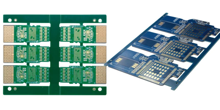
An optical module PCB traceability and MES review defines how every critical material, SMT process setting, inspection result, firmware record, and electrical or optical test result is tied to a specific module or PCBA serial number. For 400G, 800G, and next-generation 1.6T data center optics, this traceability is not only a factory reporting tool; it is part of the manufacturing control plan that helps connect high-speed channel behavior, thermal performance, optical alignment, and field-return analysis to real production evidence.
Key Takeaways
- Treat
Traceability/MESas a manufacturing evidence system, not a marketing label. It should link material lots, process parameters, inspection images, test results, rework history, and firmware configuration to a unique module or PCBA identity. - Keep 800G and 1.6T language at system-context level unless the exact module architecture, lane plan, host interface, and validation results are known. A PCB alone does not prove Ethernet compliance or optical-module interoperability.
- Use MES data to protect the high-risk interfaces: PAM4 host lanes, DSP BGA assembly, laser driver and TIA/LA placement, optical engine alignment, thermal-interface assembly, and CMIS firmware configuration.
- Do not rely on final optical test alone. SPI, AOI, X-Ray, reflow-profile capture, impedance/TDR data, power-on data, optical test, and rework logs should form one closed traceability chain.
- The RFQ package should include Gerber/ODB++, stackup, impedance tables, BOM AVL, reflow and inspection requirements, optical/electrical test points, firmware/programming rules, and serialization needs.
In This Guide
- What Traceability/MES means for optical module PCB manufacturing
- Why 800G and 1.6T optical modules raise PCB process risk
- What data should be captured in MES for each optical module PCBA
- PAM4 signal integrity, stackup, via control, and inspection evidence
- Laser driver, TIA/LA, and optical engine layout handoff
- Thermal management, TEC control, potting, and conformal coating
- SMT, selective wave soldering, SPI/AOI/X-Ray, and rework control
- CMIS firmware, module identity, and test-data traceability
- Common failure modes and what MES should help diagnose
- Cost drivers in optical module PCB manufacturing
- RFQ checklist for optical module PCB and PCBA projects
- Why choose HILPCB for optical module PCB manufacturing
- Reference standards and interface context
- FAQ
- Next steps
What Traceability/MES means for optical module PCB manufacturing
Traceability/MES for optical module PCB manufacturing is the digital record system that connects every unit to the materials, process parameters, inspection evidence, test results, firmware version, and rework events that shaped it. In a dense data center optical module, that record matters because the most expensive failures often appear only after electrical, optical, thermal, and mechanical variables interact.
A pluggable optical module PCB is not a generic high-speed board. It may carry a host electrical interface, a DSP or retimer, laser drivers, TIAs, monitoring circuits, microcontroller firmware, thermal control, and optical-subassembly connections in a very small mechanical envelope. When a unit fails BER, eye-margin, power, temperature, or optical-output tests, the useful question is not simply whether it failed. The useful question is what changed: laminate lot, copper profile, etch compensation, solder paste lot, BGA voiding, reflow profile, alignment setting, potting cure, firmware image, or test fixture.
A strong MES record turns that investigation into a controlled search instead of guesswork. It should allow an engineering team to compare a failed unit against neighboring units from the same lot, the same reflow oven run, the same component reel, the same optical-alignment station, and the same firmware release.
At board level, this review is approving a narrower statement than many articles imply. It is not claiming that the PCB alone delivers 800G, 1.6T, CMIS compliance, or system interoperability. It is saying that the manufacturing package is traceable enough to support high-speed and optical-module validation.
Traceability scope table
| MES record area | What should be captured | Why it matters for optical modules | Typical owner |
|---|---|---|---|
| Bare PCB identity | PCB serial, panel ID, stackup revision, laminate lot, copper foil type, finish, impedance coupon data | Links channel behavior and assembly yield to the actual PCB build | PCB fabrication / CAM |
| SMT process | Solder paste lot, stencil revision, SPI data, placement program, component reel IDs, reflow profile | Helps diagnose BGA solder defects, tombstoning, opens, and process drift | SMT assembly |
| BGA/QFN inspection | X-Ray images, void metrics, bridge/open detection, head-in-pillow review | Protects DSP, retimer, MCU, driver, and TIA package integrity | Quality / process engineering |
| Optical assembly | Optical engine lot, alignment parameters, adhesive or potting lot, cure profile, torque or fixture data | Helps correlate optical power and alignment drift with assembly process | Optical assembly |
| Electrical test | TDR, impedance, continuity, boundary-scan/JTAG, power rail checks, current consumption | Connects physical build quality with high-speed and power-integrity results | Test engineering |
| Optical test | Tx optical power, Rx sensitivity, BER, eye mask, wavelength, temperature sweep data | Captures the final optical/electrical behavior of each unit | Module test |
| Firmware and identity | Firmware version, CMIS configuration, serial number, vendor ID, calibration constants | Prevents misprogramming and supports field-return analysis | Firmware / production test |
| Rework history | Rework type, operator, station, date, material change, retest result | Separates clean builds from repaired units and controls risk | Manufacturing quality |
The best MES architecture is not the one that stores the most data. It is the one that stores the data needed to explain variation. For optical modules, that means linking physical process evidence to channel, optical, thermal, and firmware results.
Why 800G and 1.6T optical modules raise PCB process risk
800G and 1.6T optical module language should be handled carefully. These terms describe system and module bandwidth targets, not a standalone PCB capability claim. At PCB level, their importance is that they tighten the tolerance stack around loss, impedance discontinuity, crosstalk, connector transitions, power noise, thermal density, and manufacturing repeatability.
The move from NRZ signaling to PAM4 increased sensitivity to vertical eye margin, jitter, reflections, and crosstalk. PAM4 carries more information per symbol than NRZ, but the eye openings are smaller. That means small discontinuities that might have been manageable on slower links can become more visible in high-speed module channels.
For a PCB manufacturer and PCBA partner, the risk is not only designing a nominal stackup. It is reproducing the channel across panels, lots, and production weeks. The difference between a promising prototype and a stable module program often appears in variation: etch factor, dielectric thickness, glass weave, via stub residue, connector launch geometry, BGA solder quality, and fixture repeatability.
System context versus PCB manufacturing responsibility
| System or module term | What it signals | What the PCB/PCBA team can control | What still needs system-level proof |
|---|---|---|---|
| 400G / 800G Ethernet | High aggregate bandwidth and high-speed electrical/optical lanes | Stackup, impedance, via transitions, connector launch, material consistency, assembly quality | Ethernet PHY compliance, link interoperability, host-platform validation |
| 1.6T module planning | Next-generation bandwidth and lane-density pressure | Higher channel discipline, tighter data traceability, thermal-interface control | Final module architecture, PHY compliance, host ecosystem readiness |
| QSFP-DD / OSFP | Pluggable form factor and mechanical/electrical envelope | Connector footprint, cage interface, thermal path, module PCB fit | Complete form-factor compliance and host interoperability |
| CMIS | Management-interface and module-control context | Firmware programming, EEPROM/configuration traceability, I2C/management bus quality | Full CMIS behavior and host-management compatibility |
| LPO / CPO / NPO | Different optical-interconnect architectures | PCB process control for the selected electrical/optical interface | Architecture-level performance, interoperability, and platform validation |
A useful optical module PCB guide avoids inflated performance language. It explains how the board and assembly process reduce avoidable manufacturing variation so the module design has a better chance of passing its own validation plan.
What data should be captured in MES for each optical module PCBA
The MES data model should be designed before production starts. If serialization and data capture are added after defects appear, the most important evidence may already be missing.
Start with unit identity. Each PCB, PCBA, and finished module should have a unique ID that survives fabrication, SMT, optical assembly, firmware programming, final test, packing, and repair. For small modules, the ID may be a laser mark, 2D code, carrier ID, panel ID, or fixture-linked record. The method is less important than continuity. The record must remain unambiguous.
Then define the critical-to-quality fields. Optical modules usually need traceability at two levels: lot-level evidence and unit-level evidence. Lot-level evidence helps when a material or process batch drifts. Unit-level evidence helps when one board in an otherwise good batch behaves differently.
Recommended MES capture plan
| Stage | Lot-level fields | Unit-level fields | Engineering use |
|---|---|---|---|
| Incoming material | Laminate lot, copper foil type, solder mask lot, surface finish chemistry, component reel IDs | PCB serial or panel position | Correlate yield shifts with material lots |
| PCB fabrication | Lamination recipe, drill file revision, plating data, etch compensation, impedance coupon results | Panel position, serial, measured impedance when available | Detect stackup or etch-related SI drift |
| SMT printing | Solder paste lot, stencil ID, printer settings | SPI volume/area/height by pad for critical packages | Prevent BGA/QFN and fine-pitch defects |
| Placement | Machine program, feeder/reel, nozzle, placement verification | Component coordinates, missing/wrong-part alarms | Investigate component skew, rotation, and wrong-reel events |
| Reflow | Oven recipe, zone temperatures, belt speed, nitrogen/vacuum state when used | Profile association by carrier or lot | Correlate voiding and solder defects |
| Inspection | AOI program, X-Ray program, acceptance rule revision | Defect images, BGA void metrics, repair decisions | Provide physical evidence for quality review |
| Firmware | Firmware image, CMIS map/config, programming station | Serial number, programmed version, checksum, calibration constants | Prevent configuration escapes |
| Final test | Test station, fixture, calibration status | BER, eye, optical power, current, temperature, alarms | Tie performance to build history |
| Rework | Rework station, material, operator, profile | Defect type, action, retest result | Control repaired-unit risk |
The capture plan should also define who can change records, how record changes are audited, and which data must be exported for the customer. A traceability system that cannot explain revision changes is not traceability. It is only data storage.
PAM4 signal integrity, stackup, via control, and inspection evidence
High-speed PAM4 routing is one of the strongest reasons to use a disciplined MES workflow. The channel between the module edge connector and the DSP, retimer, driver, or optical engine can be short in physical length, but it is electrically demanding.
For the PCB, the first control point is stackup. Low-loss materials, stable dielectric thickness, copper roughness, glass style, and resin content all influence insertion loss and impedance. The chosen stackup should be frozen with the board revision, and the MES record should link every PCB serial or panel to the corresponding material lot and impedance evidence.
The second control point is transition design. Vias, BGA escapes, connector launches, backdrilling, and reference-plane changes often dominate the discontinuity budget. Backdrill depth control and residual stub management should be documented in the fabrication traveler and verified with the appropriate inspection or coupon method.
The third control point is power integrity. DSPs, retimers, drivers, TIAs, and TEC controllers can be sensitive to rail noise. PDN design therefore needs decoupling placement, plane continuity, power-domain separation, and current-return paths that are consistent with the high-speed layout.
PAM4 PCB control table
| Design or process area | Risk if uncontrolled | Board-level control | MES or inspection evidence |
|---|---|---|---|
| Low-loss laminate | Higher insertion loss or lot-to-lot channel drift | Approved stackup, laminate AVL, copper profile selection | Material lot and stackup revision record |
| Differential routing | Reflection, skew, crosstalk, eye closure | Controlled impedance, pair symmetry, reference continuity | TDR/coupon data and CAM review notes |
| Via transitions | Resonance and discontinuity from unused stubs | Backdrill, microvia, blind/buried via, optimized antipads | Drill/backdrill record, cross-section, X-Ray where relevant |
| BGA escape | Return-path gaps and dense routing defects | Ground-via stitching, fanout rules, layer transition discipline | AOI/X-Ray and electrical test data |
| Power domains | Jitter, BER degradation, optical noise coupling | PDN review, decoupling plan, analog/digital rail separation | Power-on rail data and current profile |
| Solder quality | Opens, intermittent faults, thermal resistance | SPI, AOI, X-Ray, reflow profile control | Unit-level inspection images and pass/fail logs |
A common mistake is to treat MES only as a quality-reporting tool after SMT. For high-speed optical modules, MES should begin at PCB fabrication because the channel is already being shaped by laminate, copper, drilling, plating, and etching before the first component is placed.
Laser driver, TIA/LA, and optical engine layout handoff
The Tx and Rx areas of an optical module PCB are mixed electrical, optical, and mechanical systems. The driver, laser, photodiode, TIA/LA, optical engine, and monitoring circuitry must be treated as one controlled interface rather than independent schematic blocks.
On the transmit side, the laser driver should be placed to minimize parasitic inductance and keep high-current modulation paths short. Its power network needs dense local decoupling and a clean return path. The layout should keep switching noise and driver current edges from coupling into the receiver section or management circuits.
On the receive side, the photodiode-to-TIA path is extremely sensitive. The TIA input region should be protected from digital crosstalk, power-supply noise, and unnecessary parasitic capacitance. Ground shielding, short input connections, and disciplined isolation from noisy drivers are more important than visually tidy routing.
The optical engine adds another constraint. Optical alignment, substrate CTE, board warpage, solder-joint fatigue, adhesive stress, and fiber or lens positioning can all affect module performance. The PCB does not own the entire optical path, but its flatness, pad geometry, assembly plan, and material selection can make optical assembly easier or harder.
Optoelectronic handoff checklist
| Area | Review question | Evidence to keep traceable |
|---|---|---|
| Laser driver placement | Are high-current, high-speed paths kept short and separated from sensitive Rx areas? | Placement revision, BOM lot, reflow and inspection results |
| TIA/LA input | Is the weak-signal input protected from power and digital noise coupling? | Layout review notes, AOI, power-noise test results |
| Optical engine interface | Are pad, mechanical, and warpage assumptions documented? | PCB flatness/warpage data, assembly fixture ID, alignment log |
| Adhesive or potting | Is the material compatible with stress, temperature, and optical alignment requirements? | Material lot, mix/cure profile, operator/station record |
| Module cage / housing contact | Does the board support the intended thermal and mechanical interface? | Torque data, TIM lot, assembly fixture data |
| Rework policy | Are optically aligned or potted assemblies restricted from uncontrolled rework? | Rework authorization and retest records |
This is also where supplier wording should stay modest. A PCB manufacturer can support the electrical and assembly evidence chain; it cannot independently guarantee coupling efficiency, optical sensitivity, host interoperability, or full module performance without the customer's complete optical design and test plan.
Thermal management, TEC control, potting, and conformal coating
Thermal management is a central optical module PCB challenge because high-speed DSPs, drivers, TIAs, TEC circuits, and compact housings concentrate heat in a small volume. The PCB is part of the heat path from active devices to the module case, cage, and switch airflow, but it is not the whole thermal solution.
At board level, thermal design begins with copper distribution, thermal vias, heat-spreader strategy, device placement, and TIM interface planning. If the module includes a TEC, the TEC control loop adds high-current switching, precision temperature sensing, and sensitive analog feedback. That combination requires careful separation between power-control loops and low-noise optical receive paths.
Potting and encapsulation can protect fragile optical or mechanical assemblies, but they also change stress and heat flow. Conformal coating can improve environmental resistance, but it can complicate rework, connector contact areas, optical windows, and thermal paths if masking is not controlled. MES should capture coating or encapsulation material lot, mask program, cure profile, and inspection status.
Thermal and protection control table
| Control area | PCB/PCBA design concern | MES record to keep |
|---|---|---|
| DSP and driver heat path | Thermal vias, copper planes, device-to-case conduction | PCB stackup, via design, thermal interface assembly data |
| TEC power loop | Switching current, current sense accuracy, loop stability | BOM lot, placement data, power-on current, thermal test results |
| Temperature sensing | Sensor placement and calibration | Sensor lot, calibration constants, firmware version |
| TIM assembly | Thickness, compression, torque, surface contact | TIM lot, torque or fixture record, operator/station |
| Potting / encapsulation | Stress, voiding, cure shrinkage, serviceability | Resin lot, mix ratio, dispense volume, cure time/temperature |
| Conformal coating | Moisture protection, masking, connector/optical keepouts | Coating lot, mask revision, cure record, inspection image |
Thermal performance should be validated at module or system level. The PCB review can support thermal repeatability, but it should not publish a blanket claim that a specific board construction guarantees a module power class or operating case temperature.
SMT, selective wave soldering, SPI/AOI/X-Ray, and rework control
Optical module PCBA assembly is unforgiving because the board contains fine-pitch digital devices, sensitive analog optical components, dense passives, high-speed connectors, and often mechanically sensitive optical hardware. A good inspection plan separates what each inspection step can and cannot prove.
SPI checks solder paste before placement. It helps prevent insufficient paste, excessive paste, bridge risk, and inconsistent volume on fine-pitch pads. AOI checks visible component placement and solder-joint quality. X-Ray checks hidden joints under BGA, QFN, LGA, and some connector structures. Boundary-scan/JTAG or functional test checks electrical connectivity where physical probing is not practical.
Selective wave soldering may be used when through-hole connectors or mechanically stressed pins are part of the design. It should be controlled with the same traceability discipline as SMT because poor solder fill or thermal damage at connectors can create intermittent module or host-interface faults.
Inspection coverage table
| Inspection or test step | Best at finding | Not enough to prove by itself |
|---|---|---|
| SPI | Solder paste volume, offset, bridging risk, insufficient deposit | Final joint quality after reflow |
| AOI | Missing parts, polarity errors, visible solder defects, skew | Hidden BGA/QFN solder defects |
| X-Ray | BGA voids, shorts, opens, head-in-pillow indicators, hidden joint alignment | Full high-speed channel performance |
| Boundary-scan/JTAG | Digital connectivity on inaccessible pins | Analog optical performance or solder void morphology |
| Flying probe / ICT | Opens, shorts, component presence on accessible nets | Full module operation |
| Functional test | Power rails, management interface, basic system behavior | Root cause of every physical defect |
| Optical test | BER, Tx/Rx behavior, optical power, alarm thresholds | Which process step caused a failure unless MES data is linked |
Rework must be treated as a controlled process, not a side note. A reworked BGA, optical-engine area, or potted assembly should carry a record of what changed and what retest evidence was collected. In high-value optical modules, uncontrolled rework history can destroy the usefulness of traceability.
CMIS firmware, module identity, and test-data traceability
Modern pluggable modules are managed devices. The PCB may need to support a management controller, I2C or two-wire management interface, EEPROM or flash, calibration data, temperature monitoring, power monitoring, alarms, and firmware update workflows.
CMIS belongs at module-management level. For PCB and PCBA work, the practical issue is not to claim CMIS compliance. The practical issue is to make sure the board supports the required management bus quality, power sequencing, programming access, firmware flashing, identity data, and test-data linkage.
A traceability/MES system should connect the following fields to the unit serial number:
- firmware image and version
- programming station and timestamp
- checksum or verification result
- module serial number and customer configuration
- calibration constants for power, temperature, optical monitoring, or bias current
- CMIS memory-map configuration or customer-specific data, where applicable
- final test results after firmware load
- any firmware reflash or rework event
This record prevents the classic production escape where the hardware is correct but the module carries the wrong firmware, wrong customer identity, wrong calibration data, or wrong alarm thresholds.
Common failure modes and what MES should help diagnose
A strong MES system is most valuable when it shortens failure analysis. The table below shows how optical module problems often map back to process evidence.
| Symptom | Possible PCB/PCBA contributor | MES data that helps narrow the root cause |
|---|---|---|
| BER failure or closed eye | Excessive channel loss, impedance shift, via stub, connector launch issue, BGA defect | Stackup lot, TDR/coupon data, backdrill data, X-Ray, reflow profile |
| High module current | Wrong component, rail short, firmware misconfiguration, driver bias issue | BOM reel ID, AOI, ICT/FCT, firmware version, current test data |
| Optical power drift | Laser driver issue, TEC instability, optical alignment stress, thermal path variation | Driver lot, TEC test data, alignment log, potting cure, thermal test |
| Rx sensitivity degradation | TIA input noise, crosstalk, PD/TIA assembly issue, contamination | Layout revision, AOI, cleaning/coating data, optical test trend |
| Intermittent host connection | Connector solder issue, edge contact contamination, management bus fault | Selective wave profile, AOI, connector lot, continuity test |
| Thermal shutdown | TIM thickness error, poor case contact, missing thermal via connection, excessive power | TIM lot, torque data, X-Ray, thermal inspection, power test |
| Field return with unknown history | Uncontrolled rework or missing serial linkage | Rework logs, serial record, firmware record, packing history |
The table is also a reminder that final test data is not enough. A failed unit is only useful for improvement when its test result can be traced back to the process conditions that produced it.
Cost drivers in optical module PCB manufacturing
Optical module PCB cost is driven less by board area and more by risk control. Dense, small boards can be expensive because they require premium materials, tight process windows, high inspection coverage, and traceable assembly.
| Cost driver | Why it increases cost | How to control it without weakening reliability |
|---|---|---|
| Low-loss laminate | Material cost and controlled storage/handling are higher | Use the lowest-loss material that satisfies the validated channel need, not the highest-spec option by default |
| Tight impedance and backdrill | Adds CAM review, drilling control, coupon testing, and inspection burden | Classify only true high-speed nets as critical and document requirements clearly |
| Fine-pitch BGA/QFN | Requires advanced stencil, placement, reflow, and X-Ray control | Provide accurate package data and clear X-Ray acceptance rules |
| Optical alignment and potting | Adds fixture time, cure time, and rework limitations | Define alignment data and potting requirements before NPI |
| Full serialization/MES | Adds system setup, scanning steps, and data management | Capture CTQ data first; avoid collecting low-value records that no one uses |
| Functional and optical test | Requires fixtures, calibrated instruments, and test time | Separate engineering debug tests from production pass/fail tests |
| Rework restrictions | Limits salvage options for sensitive assemblies | Design for access where rework is allowed and define no-rework zones early |
The most expensive version of traceability is the version added after a quality crisis. Building the data plan during NPI is usually cheaper than reconstructing production history after field returns begin.
RFQ checklist for optical module PCB and PCBA projects
A strong RFQ package reduces ambiguity and helps the supplier quote the correct manufacturing route instead of assuming a generic high-speed PCB.
Files and design data
- Gerber, ODB++, IPC-2581, or native design export
- Drill files, backdrill files, via stack definitions, and controlled-depth requirements
- Stackup drawing with material preference, dielectric thickness, copper weights, and copper profile notes
- Impedance table with net classes, target values, tolerance expectations, and coupon requirements
- Assembly drawing, centroid file, BOM, AVL/AML, and package drawings for critical components
- Mechanical drawing showing module outline, edge connector, cage interface, keepout zones, and thermal contact areas
High-speed and optical requirements
- Host lane speed and modulation context, such as NRZ or PAM4
- Critical channel length and connector transition notes
- BGA/retimer/DSP package details
- Optical engine interface, alignment tolerance assumptions, and fixture requirements
- Tx/Rx electrical interface notes for driver, TIA/LA, PD, laser, or optical engine
- Test point and fixture-access requirements
Manufacturing and inspection requirements
- Solder paste, stencil, and reflow constraints
- SPI, AOI, X-Ray, boundary-scan/JTAG, ICT, FCT, or optical test requirements
- BGA void criteria and hidden-joint acceptance rules
- Selective wave soldering requirements for through-hole connectors, if any
- Cleaning, ionic contamination, conformal coating, potting, or encapsulation requirements
- Rework limits and no-rework areas
MES and traceability requirements
- Serialization method and barcode/2D code location
- Required fields for material lot, component reel, process settings, inspection images, test data, and firmware data
- Customer data-export format
- Firmware programming, checksum, CMIS configuration, and calibration record requirements
- Packing, label, and customer serial-number mapping rules
Reliability and validation requirements
- Thermal cycling, high-temperature operating, vibration, shock, humidity, or storage requirements
- Module-level thermal test plan and pass/fail limits
- Optical/electrical test limits and customer test scripts
- Lot release criteria and sample size rules
- Failure-analysis and 8D reporting expectations
Why choose HILPCB for optical module PCB manufacturing
HILPCB supports optical module PCB projects by aligning high-speed PCB fabrication, precision assembly, inspection, and traceability into one manufacturing handoff. For this product class, the value is not a single capability slogan. It is the ability to keep stackup, assembly, inspection, firmware, and test records connected.
Relevant HILPCB support paths include:
- High-Speed PCB manufacturing for controlled-impedance host channels, DSP routing, and low-loss stackup review.
- HDI PCB for dense BGA escape, microvia routing, and compact module layouts.
- SMT Assembly for fine-pitch components, SPI/AOI/X-Ray inspection, and production assembly control.
- Turnkey Assembly when BOM sourcing, assembly, programming, test, and packing need to be coordinated in one flow.
- Small Batch Assembly for NPI builds where MES fields, test coverage, and rework rules still need to be proven.
The best time to involve the manufacturing team is before the first optical build. Stackup, serialization, inspection, firmware programming, and test-data format are much easier to define before the first batch than after the first failure-analysis meeting.
Reference standards and interface context
The following references are useful for engineering context. They should not be treated as proof that a PCB or PCBA alone is compliant.
- IEEE 802.3df-2024 — IEEE Ethernet amendment for 400 Gb/s and 800 Gb/s Ethernet.
- IEEE P802.3dj — IEEE project context for 200 Gb/s, 400 Gb/s, 800 Gb/s, and 1.6 Tb/s Ethernet.
- OIF CEI-112G and CEI-224G work — electrical interface context for high-speed chip-to-module and related optical-module links.
- OIF CMIS 5.3 — Common Management Interface Specification for pluggable or on-board modules.
- QSFP-DD MSA Hardware Specification — QSFP-DD form-factor mechanical, connector, thermal, pinout, and management context.
- OSFP MSA Specification — OSFP and OSFP-XD form-factor mechanical, electrical, pinout, and thermal context.
- IPC-A-610 — electronic assembly acceptance requirements.
- IPC-J-STD-001 — soldered electrical and electronic assembly requirements.
- IPC-7095 — design and assembly process implementation guidance for BGA and fine-pitch BGA.
- IPC-2221 / IPC-2222 — generic and rigid PCB design context.
FAQ
What is Traceability/MES in optical module PCB manufacturing?
Traceability/MES is the manufacturing data system that links each optical module PCB or PCBA to its material lots, process settings, inspection results, firmware version, test data, and rework history. It helps engineers connect performance variation to the actual build conditions that produced the unit.
Does MES prove that an optical module is 800G or 1.6T compliant?
No. MES supports evidence collection and process control, but it does not independently prove Ethernet compliance, optical interoperability, or host compatibility. Those outcomes require module-level and system-level validation.
Which process data matters most for PAM4 optical modules?
The most important records usually include stackup and laminate lot, impedance/TDR data, backdrill control, reflow profile, SPI data, X-Ray inspection, DSP or retimer component lot, power-rail test, BER or eye test, and firmware configuration.
Why are SPI, AOI, and X-Ray all needed?
They inspect different defect classes. SPI checks solder paste before placement, AOI checks visible placement and solder defects, and X-Ray checks hidden joints under BGA, QFN, LGA, and other bottom-terminated packages. None of them replaces high-speed or optical functional validation.
How does CMIS relate to the PCB?
CMIS is a module-management interface specification. For the PCB and PCBA team, the relevant work is supporting the management bus, programming access, identity storage, firmware version control, calibration data, and traceable configuration loading.
Should conformal coating or potting always be used on optical module PCBs?
Not always. Coating and potting can improve environmental or mechanical protection, but they may affect rework, thermal flow, optical interfaces, connectors, and stress. They should be selected according to the module design, operating environment, and validation plan.
What should be sent for a quote?
Send the Gerber or ODB++ package, stackup, impedance table, BOM, assembly files, optical interface notes, inspection requirements, firmware/programming requirements, serialization rules, and final test expectations. The more complete the RFQ package is, the easier it is to quote the correct NPI and production route.
Next steps
If your optical module PCB is moving from prototype to production, do not wait until final test to decide what data should be traceable. The most valuable MES records begin at material intake, stackup release, SMT setup, and inspection-plan definition.
Send your Gerber or ODB++ package, stackup, BOM, impedance table, optical interface notes, and MES traceability requirements to [email protected], or upload the package through the Quote page. HILPCB can review the PCB fabrication, assembly, inspection, and traceability plan before NPI so the first serious build creates usable engineering evidence instead of disconnected test results.