
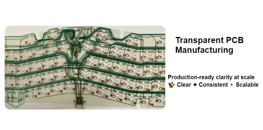
Transparent PCBs (also called clear circuit boards or see-through PCBs) enable electronics where the board must stay visually unobtrusive—such as AR/VR optics, micro-LED lighting, transparent antennas, medical imaging modules, and design-driven consumer products. Unlike standard FR4, transparent PCB manufacturing must balance optical clarity, electrical reliability, thermal stability, and process yield—often with much tighter cosmetic requirements.
This guide explains the practical manufacturing choices that determine whether a transparent PCB design can move from prototype to stable production: substrate selection, conductor patterning, via formation (including TGV), assembly constraints, optical-grade inspection, and how to qualify the right manufacturing partner.
Choosing Transparent Substrates for Real-World Reliability
The substrate is the foundation of a transparent PCB. It sets optical transmission, coefficient of thermal expansion (CTE), moisture behavior, and the process window for drilling, plating, and assembly. “More transparent” is not always better if the material cannot survive temperature cycling, bonding stress, or chemical exposure.
Transparent PCB projects typically succeed when substrate choice is made from the start based on the product’s temperature, mechanical environment, and optical tolerance—not only cost.
Key Substrate Selection Criteria
- Optical requirements: transmission targets, haze limits, and visible defect tolerance
- Thermal stability: reflow compatibility, long-term thermal cycling resistance, CTE matching
- Mechanical behavior: brittleness (glass) vs. flexibility (films), handling sensitivity
- Moisture and chemical resistance: humidity exposure, cleaning solvent compatibility
- Process compatibility: feasibility of vias, plating adhesion, and surface treatment options
- Supply stability: consistent material batches and controlled thickness tolerance
For foldable or wearable optics that demand flexing and tight thickness control, transparent film solutions can follow manufacturing logic similar to flex PCBs—with additional optical and cleanliness constraints.
Creating “Invisible” Conductors Without Losing Electrical Performance
A transparent circuit must conduct current and signals while remaining visually acceptable. That pushes manufacturers toward thin films, fine patterning, and conductor geometries that minimize visible lines—without sacrificing adhesion, resistance stability, or long-term corrosion resistance.
The manufacturing risk here is common: traces that look great initially but fail after humidity, thermal cycling, or mechanical stress due to weak adhesion or micro-cracking.
Key Conductor Patterning Techniques
- Thin-film metallization: sputtering or vacuum deposition for uniform, thin conductive layers
- Fine photolithography: tight line/space control for compact, high-resolution layouts
- Metal mesh / ultra-fine grid: reduced visual impact while maintaining conductivity
- Adhesion engineering: plasma cleaning, surface activation, and adhesion promoters
- Design rules for visibility: routing in non-viewing zones, consistent pattern density, and controlled edge effects
- Reliability validation: peel/adhesion testing and humidity aging to verify stability
When transparent circuits require dense routing (camera modules, micro-display drivers, sensor arrays), production constraints become closer to HDI PCBs—but with stricter cosmetic limits and often less forgiving substrates.
Through-Glass Via and Interconnect Strategy for Compact Optical Electronics
Compact transparent electronics often need vertical interconnects for sensor routing, LED arrays, or mixed-signal integration. For glass-based designs, through-glass vias (TGVs) are a common path—but they require specialized drilling/etching, controlled metallization, and strict dimensional management.
The key procurement reality: TGV feasibility is not just “can you drill a hole.” It depends on aspect ratio, surface preparation, plating continuity, and how the via behaves under thermal stress and potting/encapsulation.
Key TGV and Interconnect Design Practices
- Via formation method matching the material: laser drilling, etching, or hybrid approaches
- Aspect ratio control: keep designs within stable plating and fill capability
- Metallization continuity: avoid voids and thin spots that become failure points
- Stress management: via keep-outs and spacing rules to reduce crack initiation
- Interconnect architecture: single-sided vs. double-sided routing and jumper strategy
- Test access planning: continuity and isolation verification before final encapsulation
For RF-visible products like transparent antennas or window-integrated connectivity, interconnect design often includes controlled impedance planning that aligns with high-frequency PCB manufacturing discipline—while still meeting optical constraints.

Thermal Management in Transparent PCBs Without Blocking Light
Transparent substrates typically provide less thermal margin than copper-clad FR4, and many transparent applications hide electronics inside compact enclosures with limited airflow. Thermal issues show up as optical distortion, adhesive yellowing, delamination, and accelerated component aging.
A reliable thermal approach usually combines layout strategy, localized heat spreading, and mechanical integration—rather than relying on one material “fix.”
Key Thermal Management Techniques
- Thermal-aware placement: distribute hot components and avoid clustering near optical critical zones
- Heat spreading structures: use copper patterns in non-viewing zones to reduce hotspots
- Interface engineering: define heat paths to the enclosure/heatsink early
- Encapsulant planning: optically clear potting or adhesives must be thermally validated
- Process window control: reflow and cure profiles must avoid substrate warp and stress
- High-power hybrid approach: combine transparent windows with high-dissipation bases when needed
For high-power lighting or compact power modules that require strong heat extraction, hybrid builds can incorporate metal-core PCBs in non-viewing zones while preserving transparent areas where optics matter.
Assembly and Handling: What Makes Transparent PCBA Fail in Production
Transparent PCB assembly is often where projects stall: fragile substrates, optical cleanliness expectations, and reflow/curing constraints can reduce yield quickly if the process is not designed for transparent materials.
Beyond soldering, the biggest risks are scratches, particle contamination, adhesive haze, and subtle warpage that becomes visually obvious once installed behind optics.
Key Transparent PCBA Controls
- Handling and fixturing: vacuum tooling, soft contact points, anti-scratch flow
- Reflow profile tuning: lower ramp rates and controlled peak temperatures for stress reduction
- Optically clear bonding: adhesive selection that minimizes haze and yellowing over time
- Inspection adaptation: backlight and polarized imaging for transparent substrates
- Residue-free cleaning: chemistry validated to prevent haze and micro-staining
- Assembly consistency: controlled solder mask openings and pad design for stable joints
Most programs rely on disciplined SMT assembly with additional cleanliness, fixturing, and optical inspection steps tailored to transparent materials.
Quality Control Standards for Transparent PCBs
Transparent PCBs must meet electrical criteria and optical criteria. Cosmetic defects that are irrelevant on green soldermask boards can be functional failures in transparent electronics because they reduce transmission, increase haze, or appear as visible artifacts.
A practical QC plan defines measurable optical thresholds and ties them to batch-level reporting—so buyers can verify repeatability.
Key Optical and Electrical Validation Methods
- Optical transmission testing: batch verification across visible spectrum
- Haze/clarity measurement: objective haze limits tied to product requirements
- Flatness and dimensional checks: bow/twist control and feature alignment tolerance
- Continuity and isolation: including higher-voltage isolation where required
- Thermal cycling and humidity aging: to validate optical stability and adhesion durability
- Cosmetic criteria standardization: documented defect limits (scratches, particles, edge chips)
For early-stage programs, pilot runs with tight inspection feedback loops reduce redesign risk. Many teams start with small-batch assembly to validate substrate handling, optical QC limits, and assembly yield before committing to volume tooling.
FAQ
What makes transparent PCB manufacturing fundamentally different from standard FR4 fabrication?
The biggest difference is that transparent PCBs must satisfy optical requirements as well as electrical ones. Substrate handling, surface cleanliness, patterning precision, bonding methods, and inspection criteria all become more demanding because even small cosmetic or dimensional defects can affect both function and visual quality.
Why is optical quality control so important for transparent PCBs?
Because defects that might be acceptable on conventional boards can become functional or commercial failures on transparent electronics. Haze, scratches, residue, edge chips, and visible process artifacts can reduce transmission, distort appearance, or undermine the user-facing quality of displays, sensors, and other optical products.
What should teams validate before scaling a transparent PCB from pilot to production?
They should validate substrate handling, optical transmission targets, haze limits, flatness, bonding stability, cleaning compatibility, and assembly yield under real process conditions. It is important to prove not only that one sample looks good, but that the same optical and electrical standard can be repeated across batches.
What should buyers look for in a transparent PCB manufacturing partner?
They should look for experience with transparent materials, process controls adapted to optical surfaces, inspection methods beyond standard PCB QC, and a realistic path from prototype to volume. A strong partner should understand that the product is judged by what it does electrically and by how clean and stable it remains visually.
Conclusion: What to Look for in a Transparent PCB Manufacturing Partner
Transparent PCB manufacturing is not a simple variation of standard FR4 fabrication—it is a specialized process that depends on substrate physics, surface chemistry, precision patterning, optical-grade cleanliness, and inspection methods designed for transparency.
HILPCB supports transparent PCB projects with an engineering-driven workflow that prioritizes manufacturability and repeatability: substrate guidance, process selection (patterning, via strategy), assembly-ready design feedback, and optical/electrical quality controls aligned to your product’s visual and reliability targets. For teams building optical electronics that must look clean, perform reliably, and scale smoothly, choosing a manufacturing partner with transparent-material experience is one of the strongest ways to reduce schedule risk and protect yield from prototype through production.