
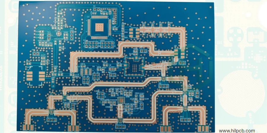
- An ultra low loss PCB is usually needed when the channel budget is driven by insertion loss, dielectric stability, copper roughness, or very high-frequency behavior rather than by ordinary rigid-board constraints.
- The first checks are channel length, operating frequency, laminate family, copper profile, via strategy, and whether the design can still meet its budget with a more ordinary material stack.
- Material selection alone is not enough. Rough copper, poor launch design, long via stubs, and weak stackup control can erase the benefit of a premium laminate.
- The right review question is not "which material has the lowest Df?" but "which material and structure meet the electrical target without overcomplicating fabrication and cost."
- A stable release path usually requires stackup, impedance model, fabrication notes, and validation method to be frozen together before the first prototype is ordered.
An ultra low loss PCB is a printed circuit board built with low-loss laminate systems and tightly controlled structures so high-speed or RF signals experience less attenuation and less distortion as they travel. It is most useful when standard FR-4 or mid-loss materials consume too much of the available insertion-loss, jitter, or phase-stability budget.
Contents
- What to review first on an ultra low loss PCB
- Key material and design rule table
- Early engineering trade-off table
- How laminate choice, copper profile, and via design interact
- How fabrication and validation should be planned
- What prototype teams should lock down before release
- FAQ
- Next steps
- References
- Author and review
What to review first on an ultra low loss PCB
An ultra low loss PCB is not just a premium-material version of an ordinary multilayer board. It is usually part of a signal path where insertion loss, return loss, skew, or phase stability are already difficult to manage. That means the board should be reviewed as a complete channel system, not as a material procurement choice.The first review points are usually:
- how much insertion loss the channel budget can actually tolerate across the required frequency range
- whether the design is limited mainly by dielectric loss, conductor loss, via structures, connector transitions, or all of them together
- which laminate family and copper profile match the signal target without creating avoidable fabrication complexity
- whether the design really needs ultra low loss construction or can still close its budget on a lower-cost stackup
- how the board will be validated through impedance, S-parameter, eye, or other electrical measurements after fabrication
For boards that are clearly operating in fast serial, RF, or microwave territory, it is often useful to compare the structure against high-speed PCB, high-frequency PCB, and Rogers PCB routes before layout freeze.
Key material and design rule table
| Rule / parameter | What to check first | Why it matters | How to verify | If ignored | | --- | --- | --- | --- | --- | | Channel-loss budget | Define the actual insertion-loss limit over frequency and path length | Material selection only makes sense relative to a real budget | SI model, link budget, or measurement target review | Expensive material decisions without electrical justification | | Laminate family | Match resin system and dielectric behavior to the frequency and channel type | Low Df alone does not guarantee the best build choice | Stackup signoff with actual laminate data | Unstable assumptions and poor channel predictability | | Copper profile | Review roughness and foil treatment together with the laminate | Conductor loss can dominate once frequency rises | Material and foil data review | Premium laminate underperforms because copper loss is ignored | | Via strategy | Control stubs, backdrill need, and layer transitions | Vias can consume major margin in low-loss channels | Launch review, transition review, simulation | Unexpected reflections and channel collapse | | Return-path continuity | Keep reference planes and transitions electrically consistent | Clean materials cannot rescue weak routing structure | Layout review and [Gerber viewer](/tools/gerber-viewer/) inspection | Mode conversion, EMI, and poor eye behavior | | Validation method | Decide how the build will be measured after fabrication | Ultra low loss claims are only meaningful if they are testable | TDR, VNA, eye, or system-validation plan | No proof that the stackup meets the target |Early engineering trade-off table
| Material / approach | Usually stronger for | Main trade-off | What to confirm early | | --- | --- | --- | --- | | Low-loss epoxy or hybrid | Faster digital channels with more familiar fabrication flow | May not leave enough margin for the hardest channels | Channel length, frequency, fabrication availability | | Hydrocarbon / ceramic-filled systems | RF and faster digital links needing lower loss and good stability | More process sensitivity than ordinary FR-4 families | Lamination flow, roughness choice, mixed-material fit | | PTFE-based systems | Microwave and mmWave paths with very low loss targets | Higher process complexity and different fabrication controls | Mechanical constraints, drilled-hole behavior, bonding system | | Standard FR-4 with stronger design discipline | Moderate-speed channels with some margin still available | Limited headroom when frequency or path length rises | Whether the channel truly needs premium laminate at all |How laminate choice, copper profile, and via design interact
Ultra low loss performance is rarely won by one variable. It usually comes from the combined effect of laminate, copper, stackup, and transitions.Three decisions usually dominate the outcome.
1. Choose material using the real frequency and path length
Some channels need lower dielectric loss because they are long. Others need it because the frequency is high or the modulation margin is tight. The right material choice depends on where the loss is coming from and how much of it the design can afford.
2. Treat copper roughness as part of the loss budget
At higher frequencies, conductor behavior matters more. A clean dielectric target can still underperform if the copper profile is too rough for the intended channel. That is why laminate choice and foil treatment should be reviewed together instead of as separate purchasing items.
3. Control transitions, not just straight traces
Many low-loss channels fail at vias, launches, or connector regions rather than in the middle of long uniform traces. Backdrill, layer transitions, anti-pad geometry, and reference continuity often decide whether the stackup benefit survives the full route.
If the project still needs a comparison between premium epoxies, hydrocarbon-ceramic systems, and RF laminates, high-speed PCB, high-frequency PCB, and Rogers PCB evaluations should be tied to the same channel model.
How fabrication and validation should be planned
Ultra low loss designs place more burden on fabrication discipline than ordinary boards. Even a good stackup can underperform if thickness control, copper profile, drilling quality, or transition geometry drift away from the modeled assumptions.The most common review points are:
- whether the chosen laminate system is compatible with the actual layer count, bonding flow, and mechanical requirements
- whether the design needs backdrill, tighter impedance control, or stronger transition review than a standard build
- whether coupon strategy, TDR, VNA, or system-level signal measurements are defined before the board is released
- whether the first build is meant to validate material choice, channel margin, or production repeatability
If the design is still early, PCB prototype, quick-turn PCB, and impedance calculator planning usually save more time than debating material names without a frozen stackup.
What prototype teams should lock down before release
The most useful ultra low loss prototype is the one that proves the actual electrical decision, not just the one that arrives quickly.A practical release checklist usually includes:
- Channel target frozen
Define insertion-loss, return-loss, skew, or eye-margin expectations in a way the prototype can validate. - Exact laminate and foil family identified
Use the intended material system and copper profile in the release package, not a placeholder label. - Transition strategy approved
Confirm via, launch, backdrill, and reference-plane assumptions before fabrication. - Measurement method defined
Decide whether the first article will be checked by TDR, VNA, eye, or system-level measurement. - Release data aligned
Keep stackup, fabrication notes, impedance assumptions, and assembly intent synchronized. A BOM viewer review helps avoid accidental substitutions that change the result.
FAQ
When does a PCB really need ultra low loss material?
Usually when channel budget, frequency range, or path length make ordinary FR-4 or mid-loss materials too lossy for the required margin.
Is low Df the only thing that matters in an ultra low loss PCB?
No. Copper roughness, via structure, launch design, and reference continuity can matter just as much as the laminate itself.
Can a premium laminate fix a weak layout?
Not reliably. A poor transition strategy or weak return-path design can waste the benefit of a low-loss material very quickly.
When should a team compare low-loss epoxy to PTFE-based materials?
Compare them when the channel budget is tight enough that material choice could change whether the electrical target is realistic, but before routing and fabrication assumptions are locked.
What should be frozen before the first prototype release?
Freeze the channel target, laminate family, copper profile, transition strategy, and the measurement method that will prove whether the design works.
Next steps
If you are planning an ultra low loss PCB, the most useful next step is usually to review the channel budget, stackup, and transition strategy together instead of choosing material in isolation.HILPCB can support that process through:
- High-speed PCB planning for faster digital channels
- High-frequency PCB review for RF and microwave signal paths
- Rogers PCB evaluation when RF-focused laminate families are part of the solution
- PCB prototype and quick-turn PCB support for early stackup validation
- Impedance calculator checks during stackup and routing review
- Request a quote when your stackup and validation goals are ready for review