
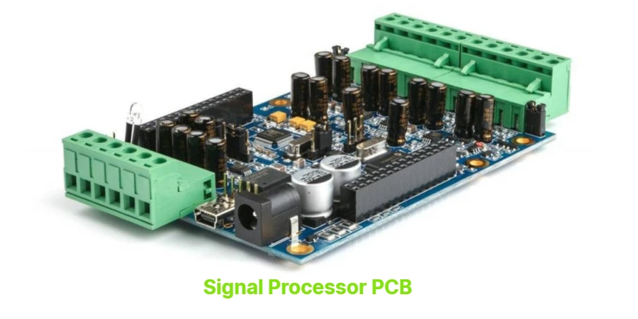
- A vector signal generator should be reviewed as a full RF signal chain, not as a generic mixed-signal PCB with a modulator added at the end.
- The first checks are modulation target, frequency range, phase-noise budget, I/Q architecture, LO distribution, shielding, and how output quality will be verified.
- Most failures show up as poor EVM, carrier leakage, image spurs, unstable output power, or disagreement between simulated and measured modulation quality.
- Material choice matters on higher-frequency paths, but DAC clocking, I/Q balance, LO isolation, grounding, and output-launch quality often decide real performance.
- Prototype success depends on freezing the validation setup early, especially when EVM, ACPR, phase noise, and modulation bandwidth must be measured repeatably.
A vector signal generator is an RF test instrument that produces modulated signals whose amplitude and phase are both controlled through I/Q signal generation. In PCB terms, that means the board has to support clean clocking, stable local-oscillator distribution, controlled RF routing, and enough isolation that digital and power noise do not corrupt the final signal.
Contents
- What to review first on a vector signal generator PCB
- Key design and validation rule table
- Early engineering trade-off table
- How I/Q generation, LO distribution, and RF layout affect output quality
- How validation should be planned before prototype release
- What prototype teams should lock down before build
- FAQ
- Next steps
- References
- Author and review
What to review first on a vector signal generator PCB
A vector signal generator is only as good as the weakest part of its signal path. Engineers usually focus on output frequency range or modulation bandwidth first, but PCB success often depends on earlier decisions: where the baseband comes from, how the DAC clock is distributed, how the LO is routed, and how much unwanted coupling the layout allows.The first review points are usually:
- what modulation formats and bandwidth the generator is expected to produce
- whether the architecture uses real-time baseband generation, stored waveforms, or a mixed approach
- how the I and Q paths are matched, filtered, and combined
- whether the LO path, clock tree, and reference distribution are protected from digital and power noise
- how the board will be validated for output power, spurs, EVM, ACPR, and phase noise after assembly
If the project includes GHz-range RF sections, it is usually worth reviewing high-frequency PCB and Rogers PCB options before routing is frozen.
Key design and validation rule table
| Rule / parameter | What to check first | Why it matters | How to verify | If ignored | | --- | --- | --- | --- | --- | | Modulation target fit | Match architecture to the real waveform families and bandwidth required | The PCB layout must support the actual modulation burden, not a generic RF source idea | System review and waveform requirement review | Overbuilt or underqualified architecture | | I/Q path balance | Keep amplitude, phase, and path symmetry under control | Imbalance raises EVM, image content, and carrier leakage | Schematic review, layout symmetry review, lab calibration | Modulation quality degrades even if RF power looks correct | | Clock and LO integrity | Protect reference clocks and LO paths from coupling and power noise | Jitter and phase noise propagate directly into output quality | Clock-tree review, shielding review, phase-noise measurement plan | Spurs, unstable phase noise, poor adjacent-channel behavior | | RF transition quality | Treat mixers, filters, amplifiers, vias, and output launches as one chain | A weak launch or transition can dominate measured performance | Layout inspection and [Gerber viewer](/tools/gerber-viewer/) review | Good core design looks bad at the connector | | Power and grounding discipline | Separate noisy digital return paths from sensitive analog and RF sections | Shared noise paths can corrupt DAC, synthesizer, and modulator behavior | PDN review, stackup review, probing plan | Random-looking distortion and repeatability problems | | Validation method | Freeze how EVM, ACPR, spurs, and power will be measured | Measurement setup determines whether prototype results are trustworthy | Test setup plan and instrument review | Lab data cannot explain board revisions clearly |Early engineering trade-off table
| Design choice | Usually stronger for | Main trade-off | What to confirm early | | --- | --- | --- | --- | | Real-time digital baseband | Dynamic standards and live modulation workflows | More clocking and digital-complexity burden | FPGA, DAC, and memory requirements | | Stored ARB-style waveform path | Repeatable lab stimulus and fixed test cases | Less flexibility for dynamic behavior | Memory depth and waveform management | | Higher integration RF chain | Smaller footprint and shorter path lengths | Harder debug and tighter thermal density | Rework access and shielding plan | | Lower-loss RF laminate | Better higher-frequency margin and output consistency | Higher cost and process sensitivity | Actual frequency plan and fabrication route |How I/Q generation, LO distribution, and RF layout affect output quality
Vector signal generator performance is usually limited by interaction across domains, not by a single component choice. The board has to carry digital baseband activity, precision clocks, synthesizer paths, mixers, filters, gain stages, and output connectors without letting one corrupt the other.Three review questions usually matter most.
1. Is the I/Q chain balanced enough for the modulation target?
I/Q mismatch does not just create a small calibration nuisance. It can directly raise image levels, worsen EVM, and create unstable behavior across frequency. The routing, filtering, gain matching, and reference-ground environment around both paths need to stay controlled.
2. Is the LO and reference network isolated well enough?
The cleanest DAC or modulator cannot recover from a noisy reference path. If the PLL, LO distribution, or reference oscillator sits too close to digital aggressors or poor return-current geometry, the output spectrum will show it. For dense layouts, high-speed PCB discipline matters even before the RF sections are evaluated.
3. Are the RF transitions treated as measurement-critical structures?
Mixers, attenuators, filters, amplifiers, and connector launches should be reviewed as one physical chain. A prototype with a mediocre launch can look like a modulation problem when the real issue is transition loss or mismatch at the board edge.
How validation should be planned before prototype release
A vector signal generator project is not ready when the schematic is complete. It is ready when the team can explain how the first build will prove output quality.The most common validation questions are:
- which measurements will define release readiness: output power, flatness, EVM, ACPR, spectral regrowth, spurs, or phase noise
- whether the prototype needs lab calibration before meaningful performance data can be trusted
- whether the measurement chain includes a spectrum analyzer, vector signal analyzer, or calibrated receiver path
- whether temperature drift, shielding changes, or enclosure effects need to be evaluated early
If the board is still in development, PCB prototype and quick-turn PCB planning usually saves more time than chasing layout tweaks without a repeatable validation workflow.
What prototype teams should lock down before build
The first article should prove the RF decision clearly. Before release, the team should know what the board is supposed to demonstrate and how lab data will be judged.A practical release checklist usually includes:
- Waveform and bandwidth target frozen
Define which standards, symbol rates, bandwidths, and modulation-quality targets the prototype needs to support. - Clock and LO plan approved
Confirm reference source, synthesizer path, shielding, and power-domain assumptions before layout release. - RF path and launch strategy approved
Treat filters, attenuators, gain stages, and connectors as part of one measured output chain. - Validation setup defined
Decide which instruments and calibration flow will be used for EVM, ACPR, spurs, and power checks. - Build revision and assembly assumptions recorded
Keep BOM substitutions, stackup, shielding parts, and tuning notes aligned. A BOM viewer review helps prevent hidden changes between lab builds.
FAQ
What is the first thing to check on a vector signal generator PCB?
Start with the modulation target, bandwidth, I/Q architecture, and the clock or LO plan. Those choices usually determine whether the rest of the PCB layout is coherent.
Why can a vector signal generator have poor EVM even when output power looks correct?
Because output power alone does not prove modulation fidelity. I/Q imbalance, phase noise, clock jitter, LO leakage, or weak isolation can all worsen EVM without obviously changing average RF power.
Does a vector signal generator always need high-end RF laminate?
Not always. It depends on frequency range, loss budget, and how much of the board is truly RF-critical. Some projects can use mixed-material or limited RF laminate regions effectively.
Why does shielding matter so much on this kind of board?
Because digital baseband activity, synthesizers, mixers, and gain stages can couple into each other easily. Good shielding and return control reduce spurs, leakage, and unstable calibration behavior.
What should be frozen before the first prototype release?
Freeze the waveform target, clock and LO architecture, RF path assumptions, measurement plan, and the exact assembly revision that the lab data will represent.
Next steps
If you are developing a vector signal generator or another RF signal-source board, the most useful next step is usually to review I/Q balance, clocking, RF transitions, and the validation chain as one system.HILPCB can support that process through:
- High-frequency PCB planning for RF signal paths and synthesizer sections
- Rogers PCB review when dielectric stability and lower loss matter
- High-speed PCB routing review when digital baseband and clock quality are part of the problem
- PCB prototype and quick-turn PCB support for early RF validation builds
- Request a quote when your stackup, RF path, and validation plan are ready for review