
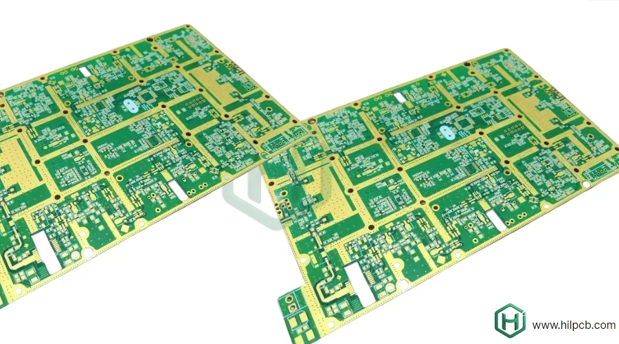
A wireless PCB integrates a radio, antenna path, digital control, power delivery, and application circuitry while preserving RF performance in the finished product. Good fabrication cannot recover a broken antenna keep-out, return path, matching network, or certification plan, so wireless success begins before layout release.
Key Takeaways
- Choose module, chip-down, or external-radio architecture before layout; each changes cost, area, RF risk, test access, and approval work.
- A 50 Ω interface is common, not universal. Use the radio, filter, switch, connector, and antenna reference impedances.
- Standard FR-4 can suit short sub-6 GHz paths when the loss budget allows. Specify Dk/Df test conditions, stackup, copper roughness, and impedance—not a material brand alone.
- Keep a continuous RF reference plane. Separating noisy circuits by placement and current path is safer than cutting a ground plane under signals.
- Antennas must be tuned and verified in the final enclosure with battery, cables, display, plastics, and nearby metal present.
- A certified radio module can reduce transmitter approval work, but the host must follow its integration conditions and still meet applicable end-product requirements.
- Pre-compliance finds risk; it is not FCC, RED, Bluetooth, Wi-Fi, Zigbee, or LoRaWAN product approval.
Module vs Chip-Down vs External Radio
Wireless architecture decision matrix
| Architecture | Best fit | Main advantage | Main risk | Evidence to request |
|---|---|---|---|---|
| Certified RF module with onboard antenna | low/medium volume, fast launch, limited RF staff | reference RF design and possible modular approval reuse | antenna clearance, host noise, approved antenna/label/integration limits | module grant/certificates, integration guide, antenna options, host-test plan |
| Module with external antenna | metal enclosure or remote antenna location | antenna placement flexibility | connector/cable loss, antenna authorization and assembly variation | connector/cable BOM, approved antenna list, conducted and OTA limits |
| Chip-down radio | high volume, tight area, custom RF or BOM target | maximum integration and unit-cost control | matching, layout, calibration and full approval burden | vendor reference design, RF simulation, tuning plan and production test |
| Separate radio board | reusable platform or mechanically isolated antenna | isolates RF redesign from main controller | board-to-board loss, grounding, emissions and logistics | interface specification, grounding, configuration and combined-product tests |
Do not select a module only by unit price. Compare module area, layer count, antenna, shielding, test time, qualification fees, engineering effort, redesign risk, supply continuity, and expected volume.
Protocol and PCB Risk Matrix
| Radio | PCB priorities | Common integration trap |
|---|---|---|
| Bluetooth LE, Zigbee, Thread at 2.4 GHz (e.g. remote controls) | compact antenna, low sleep current, clean crystal/RF supply, coexistence | placing the antenna beside USB, display clocks, metal or battery |
| Wi-Fi at 2.4/5/6 GHz | wider bandwidth, transmitter linearity, peak-current delivery, filtering and thermal margin | validating only 2.4 GHz or only one channel/data mode |
| Sub-GHz and LoRaWAN | physically larger antenna, regional band plan, matching and long-range sensitivity | copying one antenna across enclosure or regional variants without retuning |
| Cellular, LTE-M or NB-IoT | multiband antenna, high current pulses, RF exposure and operator/regional approvals | assuming module approval covers changed antenna, host and final configuration |
| GNSS | low-noise receive path, antenna bias, filtering and isolation from transmitters | routing noisy DC-DC, clocks or digital lines near the antenna/LNA path |
For collocated radios, define simultaneous operating modes, antenna isolation, coexistence control, desense targets, harmonic relationships, and worst-case transmit/receive combinations. “Each radio passes alone” does not prove the combined product works.
Stackup, RF Layout, and Antenna Release
Start from the semiconductor or module reference design, then adapt it to the actual stackup with the PCB fabricator. High-frequency PCB construction may be justified by insertion-loss, phase, stability, or frequency requirements; it is not mandatory for every IoT board.
- Route RF feeds as controlled microstrip, stripline, or grounded coplanar waveguide with a continuous adjacent reference.
- Keep the feed short and unbranched; avoid unnecessary layer changes, test pads, neck-downs, and reference-plane gaps.
- Place matching/filter parts in the vendor-recommended order and footprint. Leave tuning positions accessible without adding long stubs.
- Use return/stitching vias based on transition geometry and field containment, not a copied universal spacing rule.
- Keep switchers, crystals, high-speed buses, displays, cables, shields, fast GPIO, and noisy test fixtures away from the antenna region.
- Follow the selected antenna's exact edge position, ground length, keep-out, component clearance, and enclosure rules.
- Review solder mask, finish, etch tolerance, dielectric thickness, resin/glass construction, copper roughness, and panel orientation where they affect RF variation.
What RF Tests Prove
| Test | Strong coverage | Blind spot |
|---|---|---|
| VNA S-parameters | feed/matching return loss, insertion loss and isolation over frequency | transmitter modulation, receiver sensitivity and enclosure radiation |
| Conducted radio test | power, spectrum, harmonics, EVM/quality, sensitivity, PER/BER under defined modes | antenna efficiency, pattern, installed detuning and cable radiation |
| OTA chamber test | total radiated power, total isotropic sensitivity, efficiency/pattern or product link behavior | every field environment, network condition and software state |
| EMC/RF pre-compliance | likely emissions, immunity, exposure and band-edge risks | formal market authorization and protocol interoperability |
| Production test | assembly escapes, programmed identity and selected RF limits | complete characterization or certification of every unit |
The test plan must state bands, channels, bandwidths, data rates, power levels, antenna configuration, firmware/test mode, supply state, orientation, limits, sample size, calibration, and retest rules. Range is a system result influenced by antenna gain, orientation, enclosure, receiver, interference, protocol, data rate, installation, and environment.
Manufacturing and Assembly Controls
Wireless assembly should preserve the tuned geometry. Control board thickness and stackup, RF trace etch, antenna outline/keep-out, solder-mask registration, component substitutions, matching values, connector/cable parts, shield fit, reflow, and depanel stress. AOI and X-ray can find assembly defects but cannot prove antenna efficiency or receiver sensitivity.
SMT assembly records should link radio/module revision, crystal, filter, switch, matching components, antenna/connector/cable, firmware, inspection, rework, and RF result to the unit or lot. Any alternate in the RF path requires engineering review and may trigger retuning or compliance reassessment.
Wireless PCB RFQ Checklist
Provide these inputs for a useful quotation and engineering review:
- Design: Gerber/ODB++/IPC-2581, stackup, fabrication drawing, schematic, BOM/AVL, centroid, RF layout, impedance table, antenna and enclosure drawings
- Radio: protocol/version, bands, channels, output power, receiver target, simultaneous modes, module or chipset, approved antennas and regional variants
- Materials: laminate constraints, Dk/Df conditions, copper/finish, thickness tolerances, controlled-impedance coupon and report requirements
- Assembly: matching-value control, DNI tuning parts, shields, RF connectors/cables, MSL, programming, serialization, rework and change-notification rules
- Test: VNA ports/fixtures, conducted limits, test firmware, OTA/pre-compliance scope, production screening, data format and retention
- Commercial: prototype and annual quantity, panel constraints, target markets, certification ownership, required certificates and delivery packaging
HILPCB can review fabrication, controlled impedance, assembly access, and requested test evidence through multilayer PCB, rigid-flex PCB, SMT assembly, and turnkey assembly workflows. Final RF design, antenna tuning, firmware, exposure assessment, regulatory authorization, protocol qualification, interoperability, and product performance remain with the responsible product manufacturer and designated laboratories.
Reference Standards and Programs
- 47 CFR Parts 2 and 15, including 47 CFR 15.212 — U.S. Federal Communications Commission
- Radio Equipment Directive 2014/53/EU — European Union
- Bluetooth Core Specification and Bluetooth Qualification Program — Bluetooth SIG
- IEEE 802.11 and Wi-Fi CERTIFIED programs — IEEE and Wi-Fi Alliance
- IEEE 802.15.4 and applicable Zigbee/Thread certification programs — IEEE and relevant alliances
- LoRaWAN specifications and certification program — LoRa Alliance
- IPC-2221, IPC-6012, IPC-A-600, J-STD-001 and IPC-A-610 — IPC
Confirm current editions, regional spectrum rules, device category, antenna conditions, RF-exposure requirements, cybersecurity obligations, test methods, and responsible-party duties for each market.
Frequently Asked Questions
Does a certified wireless module certify the final product?
No. It may support modular approval reuse when integration conditions are met. The host, antenna, labeling, RF exposure, digital emissions, simultaneous transmitters and target-market rules still require review and testing.
Does every wireless PCB need Rogers material?
No. Use the loss budget and stackup analysis. Short 2.4 GHz or other sub-6 GHz paths often work on suitable FR-4; longer, wider-band or higher-frequency paths may justify lower-loss material.
Should RF and digital grounds be split?
Usually not beneath signal paths. Partition placement and current loops while preserving continuous return planes. Follow the radio vendor's reference design and verify the complete stackup.
Can antenna performance be approved on a bare PCB?
Not finally. The enclosure, battery, cables, display, user, mounting and nearby metal can detune the antenna. Tune and verify the assembled product.
What should production RF testing measure?
Measure the smallest set that reliably catches assembly and programming escapes, such as calibrated transmit power or receive response at selected frequencies. Production screening does not replace characterization or certification.
Release the Radio as a System
A wireless PCB is ready when the architecture, stackup, antenna environment, coexistence modes, conducted/OTA evidence, compliance path, production screen, and change triggers agree. Send HILPCB the RF evidence plan with the manufacturing package so cost and buildability decisions do not silently change the radio.