
IC Substrate PCB (ABF/BT) | Fine-Line SAP, Stacked Microvias, 0.25–0.40 mm Pitch
Organic IC substrates for advanced packaging: Semi-Additive Process (SAP) 15–20 μm line/space, stacked microvias 25–50 μm, ABF/BT build-up, flip-chip ready with controlled warpage and impedance ±5%.
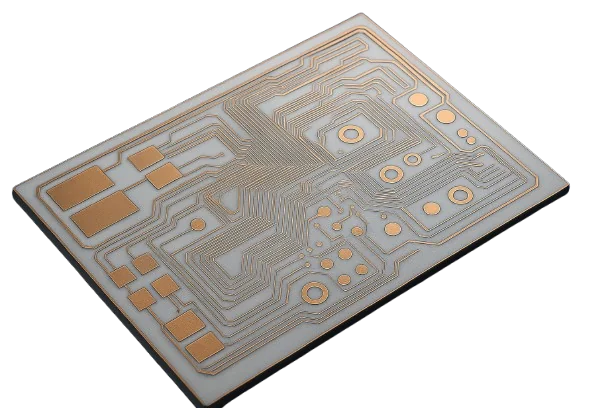
IC Substrate Manufacturing & Material Architecture
Bridging silicon I/O density with system-level reliabilityIC substrates merge semiconductor packaging and PCB technology to achieve near-silicon routing density. The Semi-Additive Process (SAP) deposits copper on a seed layer to form fine features, delivering 15–20 μm line/space with minimal undercut—typically a 2–4× density gain compared to subtractive HDI. See our HDI PCB overview and advanced HDI manufacturing notes for related build-up concepts.
ABF (Ajinomoto Build-up Film) layers of 30–60 μm maintain tight thickness control to stabilize impedance and PDN loop inductance.
BT resin composites typically show X-Y CTE of 12–14 ppm/°C, bridging silicon ~2.6 ppm/°C and FR-4 ~16–18 ppm/°C. For mixed RF/digital layouts, material choices align with our high-frequency PCB guidance and materials primer.
Critical Risk: Mis-registration between ABF layers, poor copper adhesion, or uncontrolled warpage during lamination can lead to open circuits, via cracking, or impedance drift > ±10 percent. Inadequate via-in-pad filling and surface planarity also compromise wire-bonding reliability in SiP and flip-chip assemblies.
Our Solution: We apply signal integrity simulation and backplane PCB correlation methods to validate high-density interconnect behavior. SAP and mSAP lines operate in class 1000 cleanrooms with step-coverage control below ±2 μm. Each substrate lot undergoes CTE mapping, warpage profiling, and TMA verification to IPC-6012 Class 3 AABUS requirements. Where RF front-ends demand ultra-low-loss performance, hybrid ABF and PTFE systems are co-processed to minimize dielectric discontinuity.
For further insight into material trade-offs and reliability modeling, review thermal stress validation and ceramic substrate PCB options that extend IC substrate technology into high-power RF and sensor applications.
- Fine-line routing via SAP with reduced undercut vs. subtractive etch
- ABF build-up 30–60 μm dielectric control
- Composite CTE optimization (substrate target 9–14 ppm/°C)
- Warpage control ≤0.5% of diagonal (process target)
- Impedance stability with ±5% tolerance
🚀 Quick Quote Request
📋 Get Full Capabilities
Controlled SAP Flow & Yield-Driven Quality Gates
Photolithography, plating and metrology tuned for fine pitchProcess windows are significantly tighter than standard PCB. Seed-layer deposition uniformity within ±10% precedes photo patterning for 15–20 μm features. Pulse-reverse plating manages edge growth and throwing power; differential etch removes seed between traces with width control ±10%. Microvias at 25–50 μm diameter achieve depth control ±5 μm. See manufacturing excellence and HDI process controls.
AOI at ≤5 μm resolution, X-ray registration targets, and IST (Interconnect Stress Test) over 200–500 cycles protect reliability. For board-level integration (backplanes/line cards), see backplane PCB and high-speed PCB capabilities.
- Seed-layer thickness and uniformity SPC
- Pulse-reverse copper plating for uniform features
- Laser microvia formation and copper fill verification
- AOI/X-ray/IST multi-gate quality control
IC Substrate Technical Specifications
Fine-line, stacked microvias, and flip-chip compatible build-ups
| Parameter | Standard Capability | Advanced Capability | Standard |
|---|---|---|---|
Layer Count | 4–16 layers | Up to 50 layers | JEDEC |
Base Materials | BT resin, High-Tg FR-4 | ABF, Polyimide, Glass substrate | IPC-4101/4103 |
Board Thickness | 0.20–0.80 mm | Down to 0.10 mm | IPC-A-600 |
Copper Weight | 12–18 μm | 5–35 μm (SAP builds) | IPC-4562 |
Min Trace/Space | 25/25 μm (1/1 mil) | 15/15 μm (0.6/0.6 mil) | IPC-2226 |
Min Hole Size (Laser) | 50 μm (2 mil) | 25 μm (1 mil) | IPC-2226 |
Via Technology | Microvias, buried vias | Stacked microvias, via-in-pad, any-layer HDI | IPC-6012 |
BGA Pitch | 0.40 mm | 0.25 mm | JEDEC |
Impedance Control | ±10% | ±5% with TDR | IPC-2141 |
Surface Finish | ENIG, OSP | ENEPIG, Electroless Ni/Au, Soft/Hard Gold | IPC-4552/4556 |
Quality Testing | AOI, E-test | SEM, Cross-section, TDR/IST | IPC-9252 |
Certifications | ISO 9001, UL | IATF 16949, JEDEC methods | Industry standards |
Lead Time | 15–25 days | Consult for expedite | Production schedule |
Need capabilities beyond this product? Explore our full manufacturing capabilities
Ready to start your PCB project?
Whether you need simple prototypes or complex production runs, our advanced manufacturing capabilities ensure excellent quality and reliability. Get your quote within 30 minutes.
Signal Integrity & PDN Co-Design
At 28–112 Gbps SerDes, discontinuities at ball-to-substrate transitions dominate loss and reflections. Antipad tuning and ground-via fences within 0.5–1.0 mm maintain return paths. Material Df selection (typical ABF 0.010–0.015 at 10 GHz) and copper roughness (Ra ≤1.5 μm) support insertion-loss targets—see impedance control and TDR testing.
PDN targets below 1–10 mΩ at up to 100 MHz rely on thin dielectrics 30–60 μm and dense via farms under the die (typically 100–200 vias/cm²). For board-level channels and connectors, align with our high-speed PCB and backplane PCB capabilities.
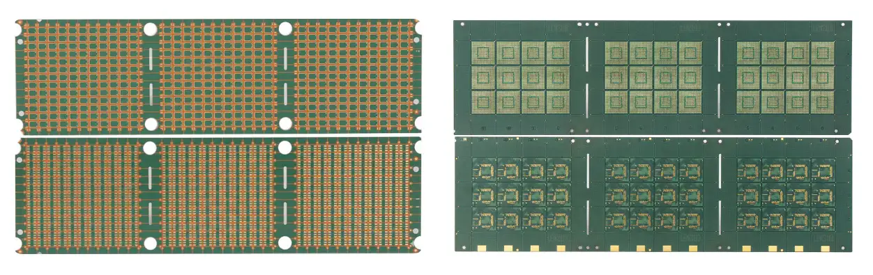
Registration Accuracy & Cleanroom Process Discipline
SAP starts with micro-roughening (Ra ~0.5–1.0 μm), seed copper 0.5–1.0 μm and resist thickness 15–25 μm for 15–20 μm patterns. Pulse-reverse plating builds signal copper 10–15 μm and planes 20–30 μm. After resist strip, differential etch clears seed without undercut. Cleanrooms (Class 1,000–10,000) minimize shorts/opens in fine pitch; see manufacturing flow.
Layer-to-layer registration targets ±25 μm using optical alignment and X-ray fiducials. Sequential build-up uses low-flow systems (resin flow <5%) to hold dielectric thickness ±5%. SPC maintains Cpk ≥1.33 for critical features.
ABF vs. BT vs. Glass & Emerging Options
ABF: photoimageable, microvia by lithography to 15–25 μm, Dk ~3.2–3.4, Df ~0.010–0.015 at 10 GHz.
BT: cost-effective for wire-bond/moderate flip-chip with X-Y CTE 12–14 ppm/°C.
Glass substrate: CTE ~3 ppm/°C and ultra-smooth Ra <0.1 μm, enabling TGV/bridge structures. For RF front-end modules, also consider ceramic PCB interposers.
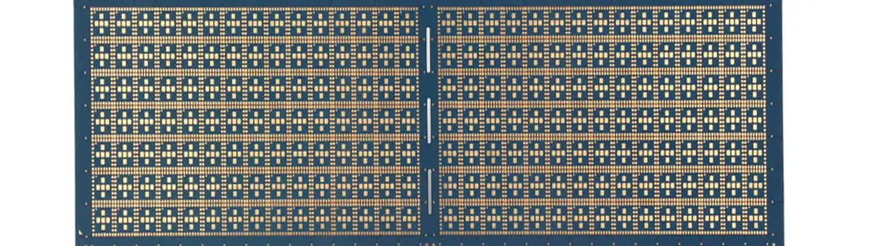
Flip-Chip, Underfill & PoP Assembly
Flip-chip requires coplanarity control; warpage exceeding 50–75 μm risks non-wet joints. Underfill with CTE 25–35 ppm/°C redistributes stress. For PoP and SiP, coordinate pitch/warpage and reflow profiles. Explore packaging notes in flip-chip substrate and system validation in box build.
Engineering Assurance & Certifications
Experience: volume SAP builds with 15–20 μm routing and 0.25–0.40 mm pitches.
Expertise: seed uniformity, pulse-reverse plating, stacked microvia fill and X-ray registration; SPC keeps Cpk ≥1.33.
Authoritativeness: JEDEC-aligned reliability, IPC-6012 Class 3 documentation.
Trustworthiness: MES traceability linking supplier lots, serialization and AOI/X-ray/IST/TDR reports.
- Controls: thickness mapping, etch factor, registration, copper roughness
- Traceability: lot codes, unit serialization, digital traveler
- Validation: IST 200–500 cycles, cross-sections, SIR, TDR
Frequently Asked Questions
ABF vs. BT: which dielectric should I choose?
What fine-line and via sizes do you support?
How do you manage warpage for flip-chip?
Can the substrate handle 112 Gbps channels?
Which surface finish is recommended?
Experience Advanced PCB Manufacturing Excellence
From simple prototypes to complex production runs, our world-class factory delivers superior quality, fast turnaround and competitive pricing. Join thousands of satisfied customers who trust us with their PCB manufacturing needs.