
Single & Double Layer PCB Manufacturing | Fast Quotes for Standard 1-2 Layer FR-4 Boards
Single-sided and double-sided FR-4 boards for low-density designs, fast prototypes, and stable repeat builds. Use this page when routing fits 1-2 layers, BOM risk is low, and you want a quote-ready path with DFM review, AOI, electrical test, and a clear upgrade route to multilayer when density grows.
Capabilities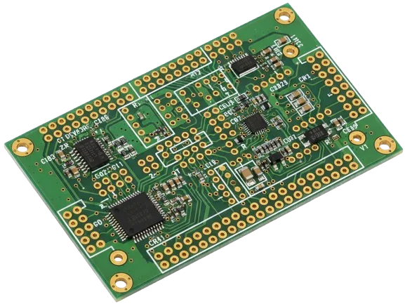
Best for Simple, Cost-Sensitive Designs
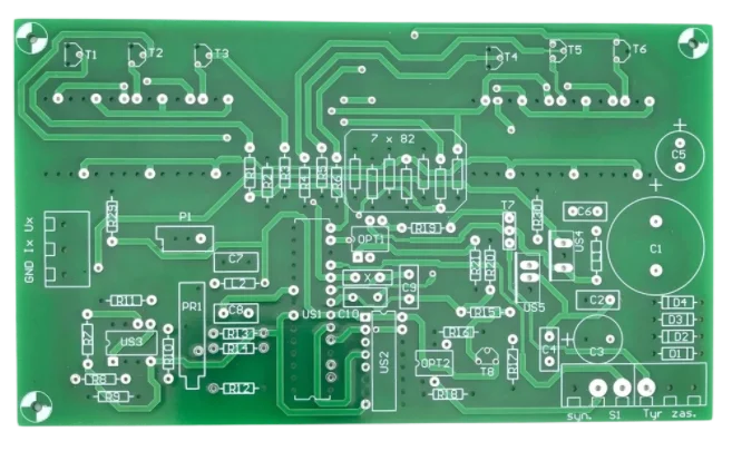
Pick 1-2 layers when routing stays simple and cost mattersSingle-sided boards are the simplest route for low-density circuits. Double-sided boards add routing freedom through plated through-holes and are a better fit when connectors, power paths, or a little extra component density force you off one side. If your layout still fits a standard FR-4 stackup, this page is the right starting point for a quote-ready build.
Compared with multilayer designs, 1-2 layer boards usually mean fewer fabrication steps, lower quote risk, and a more direct path to quick-turn production. Typical use cases include LED drivers, simple sensors, power supplies, relay boards, and industrial control modules. When routing density, impedance control, or EMI pressure grows, move to FR-4 PCB, multilayer PCB, or HDI PCB instead of forcing the design into a commodity 1-2 layer frame.
What to send for a quote: Gerber files, drill files, board outline, stackup or thickness target, finish preference, quantity, and any assembly notes. That lets us check whether the board is still a good 1-2 layer fit before we price it.
What we check first: spacing, hole sizes, finish choice, copper distribution, and whether the board will remain stable through AOI and electrical test. If the answer is no, we flag the next better family early rather than letting the job drift into avoidable rework.
- Best fit: low-density circuits, stable BOMs, and quote-driven production
- Standard FR-4 path with a clear upgrade route to multilayer or HDI
- AOI and electrical test available for production control
- Finishes: HASL, OSP, ENIG; choose by assembly and shelf-life needs
- Works well for LED drivers, sensors, power supplies, and controls
🚀 Quick Quote Request
📋 Get Full Capabilities
Process Control for Quote-Ready Builds
Keep the job simple enough to build cleanly the first timeWe verify laminate, copper weight, solder mask, and board outline before release so the build matches the quoted process. Imaging and etch control keep line geometry consistent, while AOI and electrical test catch opens, shorts, and registration issues before the board moves downstream.
For higher confidence builds, the same workflow can be paired with lot traceability and retained records. If the design later needs tighter routing, higher layer count, or stronger impedance control, the handoff path to multilayer or HDI stays straightforward because the starting data is clean.
- Registration and etch control checked before release
- Panel-level AOI; optional 100% electrical test
- Bed-of-nails or flying-probe selection by volume
- Lot traceability and retained records
- Quick-turn lanes for urgent prototypes
Technical Specifications for Single & Double Layer PCBs
Capabilities for simple, quote-ready 1-2 layer builds
| Parameter | Standard Capability | Advanced Capability | Standard |
|---|---|---|---|
Layer Count | 1–2 layers | Up to 40 layers via multilayer path | IPC-2221 |
Base Materials | FR-4 Tg 130–170 °C | Low-loss, Rogers, ceramic | IPC-4101 |
Board Thickness | 0.40–3.20 mm | 0.20–6.00 mm | IPC-A-600 |
Copper Weight | 0.5–3 oz (17–105 μm) | Up to 20 oz (heavy-copper path) | IPC-4562 |
Min Trace/Space | 150/150 μm (6/6 mil) | 75/75 μm (3/3 mil) | IPC-2221 |
Min Hole Size | 0.15 mm (6 mil) mechanical | 0.075 mm (3 mil) laser (HDI path) | IPC-2222 |
Via Technology | Through-hole | Blind/buried, via-in-pad via HDI PCB | IPC-6012 |
Max Panel Size | 571.5 × 1200 mm | 609.6 × 1219 mm | Manufacturing capability |
Impedance Control | ±10% | ±5% with TDR | IPC-2141 |
Surface Finish | HASL, OSP, ENIG | ENEPIG, Hard/Soft Gold | IPC-4552/4556 |
Quality Testing | AOI, sample E-test | 100% E-test, X-ray/ICT as needed | IPC-9252 |
Certifications | ISO 9001, UL | IPC Class 3, IATF 16949, AS9100 (on request) | Industry standards |
Lead Time | 24–48 h prototypes; 5–7 days standard | Same-day express (case by case) | Production schedule |
Ready to start your PCB project?
Whether you need simple prototypes or complex production runs, our advanced manufacturing capabilities ensure excellent quality and reliability. Get your quote within 30 minutes.
At a Glance: When 1–2 Layers Fit Best
Choose this page when the board is simple enough that extra layers would not materially improve routing, cost, or performance. It is a good fit for low-density control boards, LED drivers, basic sensor boards, simple power supplies, and repeat builds with stable BOMs.
- Good fit: simple routing, low layer count, standard FR-4, fast quote cycle
- Not the best fit: dense BGAs, tight impedance control, heavy cross-talk constraints, or aggressive EMC targets
- Quote inputs: Gerber, drill, outline, thickness, finish, quantity, and target lead time
- Next step if density grows: move to FR-4 PCB, multilayer PCB, or HDI PCB
Design Rules That Keep 1–2 Layer Boards Quote-Ready
Keep spacing consistent, avoid acid traps, and use teardrops on critical plated through-holes. Double-sided routing benefits from ground pours when EMC or thermal spreading matters, but the goal is still a simple build that the fab can execute without surprises.
- Prefer standard FR-4 unless a special material is truly required
- Keep pad and hole data clean so DFM checks can confirm manufacturability
- Choose finish based on assembly process and shelf-life needs
- Use SMT assembly or through-hole assembly only when the build really needs it
Need Expert Design Review?
Our engineering team provides free DFM analysis and optimization recommendations
Manufacturing Flow and Review Points
Flow: laminate prep → image → etch/strip → drill/plate → mask/silkscreen → finish → AOI/E-test. The review points that matter most are trace/space, drill plan, copper balance, finish choice, and whether the board should stay in the 1-2 layer lane at all.
If the data shows the design is really a multilayer candidate, we would rather say that early than force a poor-fit build into a commodity board format.
Choose This Page vs FR4, Multilayer, and HDI
- Single/Double Layer PCB: use when routing is simple, cost matters, and the board still fits a 1-2 layer build. Do not use it when you need dense routing, tighter impedance control, or microvias.
- FR-4 PCB: use when material choice is the main decision and you still need a standard PCB path. Do not use it when you are specifically deciding a low-complexity 1-2 layer build.
- Multilayer PCB: use when routing density, signal integrity, or power distribution require more layers. Do not use it when the board is simple enough to stay in 1-2 layers.
- HDI PCB: use when fine-pitch BGAs, blind/buried vias, or microvia escape routing drive the design. Do not use it when the layout still fits standard through-hole routing.
Material Options Balancing Performance and Cost
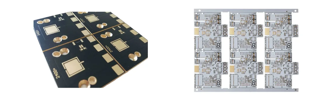
Standard FR-4 covers most cases. If higher thermal margin is needed, choose the material grade deliberately rather than leaving it implicit. For RF or ultra-low loss, move to Rogers PCB; for extreme heat paths consider metal core PCB; if flexing is required, evaluate flex PCB.
Quality Control Systems Ensuring Consistent Performance
AOI screens opens, shorts, and mask issues; flying-probe or fixture testing provides continuity and isolation checks. Documentation and retained samples support audits under ISO 9001, and lot traceability helps tie any issue back to a specific build record.
Strategic Cost Management Without Compromising Quality
Panel utilization is still a major cost driver, but the larger win is staying in the right product family. If the layout can stay in 1-2 layers, you avoid unnecessary complexity; if it cannot, it is usually cheaper to move up to the right layer count than to fight the board. That is why the quote process should answer the family question first.
Ready to optimize your PCB costs?
Get detailed cost analysis and maximum value recommendations
Typical Applications and Upgrade Triggers
Consumer devices, industrial controls, LED lighting, and simple power boards are common 1-2 layer use cases. If the design starts needing denser routing, stronger EMC isolation, or more power/ground structure, move to multilayer PCB. If the board is part of a larger system, hand off to box build after the board is stable.
Engineering Assurance & Certifications
Experience: single and double-sided programs with stable quote-to-build flow.
Expertise: controlled etch, registration, finish selection, and test coverage for simple boards.
Authoritativeness: workflows aligned to IPC Class 2/3 and ISO 9001.
Trustworthiness: MES traceability connects lot IDs to AOI and E-test results; documentation is available on request.
- Controls: etch factor, solder mask clearance, copper thickness
- Traceability: digital traveler and lot records
- Validation: AOI, E-test, microsections when needed
Frequently Asked Questions
When should I choose single-sided versus double-sided PCB?
What finishes do you recommend for 1–2 layer boards?
How fast can you deliver prototypes?
How do I keep costs low without hurting yield?
Can you migrate my design to multilayer/HDI if density grows?
What files should I send for a quote?
Experience Advanced PCB Manufacturing Excellence
From simple prototypes to complex production runs, our world-class factory delivers superior quality, fast turnaround and competitive pricing. Join thousands of satisfied customers who trust us with their PCB manufacturing needs.