
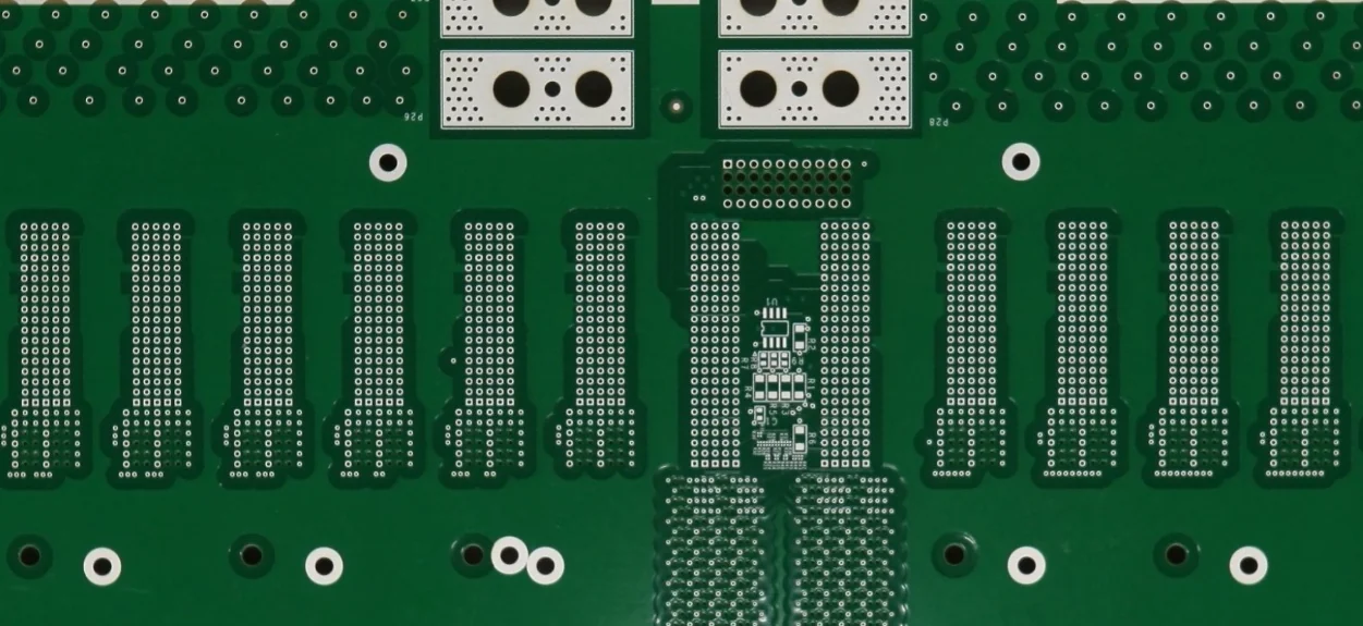
22 layer PCBs are predominantly found in applications where failure is not an option and the consequences of a defective board range from mission loss to loss of life: aerospace avionics, defense radar and electronic warfare systems, space-qualified satellite electronics, and Class III medical devices including implantable systems and surgical robots. At this layer count, the manufacturing focus shifts from pure interconnect density to absolute reliability—every via, every trace, every dielectric layer must meet the most stringent quality standards in the electronics industry.
What distinguishes high-reliability 22 layer fabrication from commercial-grade multilayer manufacturing is not a single process change but a comprehensive quality system that touches every step: incoming material inspection with lot-level traceability, certified operator training, cleanroom processing environments, coupon-based destructive testing at defined intervals, First Article Inspection documentation, and statistical process control on every critical parameter. The board itself may look identical to a commercial-grade equivalent—the difference is in the evidence that proves it was manufactured correctly.
Defense primes in the United States, avionics companies across Europe, and ISO 13485-certified medical device manufacturers in Ireland and Germany depend on HILPCB for high-reliability multilayer fabrication with full AS9102 First Article documentation—because our quality system provides the evidence trail that their regulatory and contractual requirements demand.
HILPCB Manufacturing Capability: We fabricate 22 layer PCBs to IPC-6012 Class 3/3A standards with full material traceability from raw material through finished board, coupon-based qualification testing, cleanroom processing, and controlled production environments meeting aerospace, defense, and medical quality requirements.
In This Guide
- High-Reliability Applications That Demand 22 Layers
- IPC Class 3 vs. Class 2: What Changes in Manufacturing
- Material Qualification, Selection, and Traceability
- Stack-Up, Lamination, and Aspect Ratio Challenges at 22 Layers
- Extreme-Environment Material Options
- Qualification Testing: Coupons, Microsections, and IST
- Process Controls and Environmental Requirements
- 22 Layer Boards with HDI, High-Frequency, and Rigid-Flex
- Why High-Reliability Programs Choose HILPCB
High-Reliability Applications That Demand 22 Layers
### Aerospace AvionicsFlight management computers, radar processing units, and electronic flight instrument systems require 22 layers to accommodate multiple high-speed processors with redundant power systems and extensive built-in-test (BIT) circuitry. These boards operate in temperature extremes (-55°C to +125°C), vibration environments (10-2000Hz random), and altitude-induced pressure changes—stresses that expose any manufacturing weakness in via plating, lamination bond, or copper adhesion.
Defense Electronics
Electronic warfare (EW) receivers, signals intelligence (SIGINT) processors, and fire control systems combine wideband RF front-ends with massive digital processing arrays. 22 layers provide the layer budget for both domains, with additional layers for extensive power filtering, electromagnetic shielding, and redundant signal paths required by military specifications.
Space Electronics
Satellite communication payloads and space-based computing must survive launch vibration (20G random), orbital thermal cycling (-180°C to +150°C), and radiation exposure—all without repair. Every manufacturing defect tolerable in commercial electronics becomes mission-ending in space. IPC-6012 Class 3A (Space Addendum) applies additional requirements beyond standard Class 3.
Critical Medical Devices
Class III medical devices—implantable defibrillators, surgical robots, life-support ventilator controllers—require ISO 13485-compliant manufacturing with full lot traceability and accelerated lifetime testing to ensure reliability over 10-20 year device lifetimes.
IPC Class 3 vs. Class 2: What Changes in Manufacturing
IPC-6012 defines the performance requirements. Class 3 imposes the most stringent acceptance criteria:| Parameter | Class 2 (Standard) | Class 3 (High Reliability) |
|---|---|---|
| Min. annular ring (internal) | 25μm (1mil) | 50μm (2mil) |
| Min. via plating thickness | 20μm | 25μm |
| Copper voids in via barrel | ≤10% of barrel length | 0% (no voids permitted) |
| Conductor width reduction (max) | 30% | 20% |
| Laminate voids | ≤1% of area | 0% (no delamination) |
| Solder float test | 10s at 288°C, 1 cycle | 10s at 288°C, 6 cycles |
| Bow and twist | ≤1.5% | ≤0.75% |
Class 3A (Space and Military Addendum)
For space flight hardware and critical military applications, additional requirements include: 100-500 thermal cycles (-55°C to +125°C) with no resistance increase >5% on test coupons, NASA ASTM E595 outgassing compliance (TML ≤1.0%, CVCM ≤0.10%), maximum surface ionic contamination of 1.5μg/cm² NaCl equivalent, and enhanced microsection requirements at 45° angles.
The Annular Ring Challenge at 22 Layers
Maintaining 50μm minimum annular ring on all 22 inner layers requires ±2mil (50μm) layer-to-layer registration accuracy—achievable only with optical alignment during lamination and pin-registration tooling with tight-tolerance holes. Standard registration of ±3mil is insufficient for Class 3 compliance at this layer count.
Material Qualification, Selection, and Traceability
### Incoming Material InspectionBefore any material enters production, it undergoes documented incoming inspection:
- Laminate/prepreg: Lot number recording, IPC-4101 spec verification, Tg measurement by DSC (Differential Scanning Calorimetry), resin flow testing
- Copper foil: Thickness measurement, tensile strength test, peel strength on test lamination
- Chemistry: Plating bath analysis, desmear concentration verification, etchant composition check
Qualified Material Options for 22 Layers
| Material Category | Products | Key Specification | Application |
|---|---|---|---|
| High-Tg FR-4 | Isola 370HR, ITEQ IT-180A | Tg ≥170°C | General high-reliability |
| Polyimide rigid | Isola P95, Arlon 85N | Tg ≥250°C | Military, space, extreme temp |
| Cyanate ester | Arlon 55NT | Df <0.005, low moisture | Space, high-frequency hi-rel |
| Low-loss | Megtron 6, I-Speed | Df <0.006 | High-speed digital hi-rel |
Full Lot Traceability
Every panel manufactured is assigned a unique lot/serial linking to: laminate manufacturer, lot, and date code; prepreg lot and style; copper foil supplier and batch; drill bit batch; plating chemistry batch; and all process parameter records. This traceability enables root cause analysis if a field failure occurs—the specific materials and process conditions can be identified and investigated.
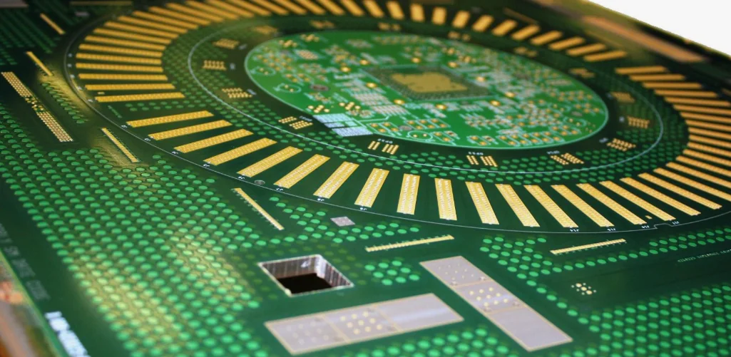 Cross-section microsection of a 22 layer PCB via barrel showing uniform copper plating thickness ≥25μm with zero voids—the IPC-6012 Class 3 acceptance criterion that HILPCB verifies on dedicated coupon structures for every production lot. This level of via plating quality is essential for aerospace, defense, and medical applications where in-field repair is impossible and a single via failure can cause mission-critical system shutdown.
Stack-Up, Lamination, and Aspect Ratio Challenges at 22 Layers
### Stack-Up DesignA 22 layer board typically provides 12-13 signal layers, 4-5 ground planes, and 4-5 power planes. Total thickness is 2.8-3.5mm. This creates significant aspect ratio constraints: a 3.0mm board with 0.3mm vias has an aspect ratio of 10:1, at the limit for reliable copper plating.
High Aspect Ratio Plating Solutions
At aspect ratios of 8:1 to 12:1, electroless copper coverage on via walls becomes uneven—the barrel center receives less chemical exposure than the entries. Solutions include:
- Extended desmear and activation (50-100% longer than standard)
- Modified electroless copper with enhanced throwing power
- Pulse plating (alternating forward and reverse current) for uniform barrel coverage
- Specifying minimum 0.25-0.3mm finished holes to reduce aspect ratio
Lamination Approach
Single-press lamination of 22 layers simultaneously is challenging due to temperature uniformity across the thick stack and simultaneous resin flow from many prepreg layers. Most fabricators use a combination approach: laminating the inner 14-16 layers in a primary press cycle, then adding 3-4 buildup layers per side in secondary cycles—each controlled with its own temperature and pressure profile.
Extreme-Environment Material Options
### High-Temperature Polyimide Rigid LaminatesFor 22 layer boards operating at 200-260°C continuously—downhole oil/gas logging equipment, jet engine health monitoring—pure polyimide rigid laminate (Tg >250°C) provides Z-axis stability and copper adhesion at temperatures that destroy standard FR-4. Cost is 3-4× standard FR-4 but justified by eliminating field failures in extreme thermal environments.
Cyanate Ester for Space Applications
Cyanate ester resins (Arlon 55NT) provide extremely low moisture absorption (<0.5% vs. 1-2% for FR-4)—critical for space-qualified boards where outgassing and moisture-induced dimensional changes must be minimized. Cyanate ester also offers lower Df (0.005 at 1GHz) than FR-4, benefiting signal integrity on the many inner stripline layers.
Thermal Management at 22 Layers
For high-power components, thermal via arrays and heavy copper inner layers (2-3oz) provide the primary heat dissipation path. Dense thermal via fields beneath power devices transfer heat to inner copper planes that act as lateral heat spreaders. For extreme thermal loads, metal core integration provides additional thermal capacity.
Qualification Testing: Coupons, Microsections, and IST
### Coupon-Based Destructive TestingDedicated test coupons embedded in the panel border undergo destructive testing that represents production board quality:
- Microsection coupons (4-6 per panel): Cross-sectioned at 200-500× magnification. Verify via plating thickness (≥25μm), zero copper voids, dielectric thickness, registration accuracy.
- Thermal stress coupons (2-4 per panel): 6 cycles of 10-second immersion at 288°C solder. Post-stress microsection verifies no delamination, cracking, or pad lifting.
- Impedance coupons (8-12 per panel): TDR-measured for all unique impedance geometries.
- Peel strength coupons: Copper-to-laminate adhesion ≥8 lb/in internal, ≥6 lb/in on treated surfaces.
- IST coupons (for Class 3A): 200-500 rapid thermal cycles with continuous resistance monitoring.
First Article Inspection (FAI)
Every new part number undergoes comprehensive FAI per AS9102 format, documenting all coupon results, dimensional measurements, and photographic evidence. The FAI package is archived as the baseline for production monitoring—any future production lot is compared against the FAI baseline to detect process drift.
Acceptance Criteria Summary (IPC-6012 Class 3)
| Test | Criterion |
|---|---|
| Via plating | ≥25μm average, zero voids |
| Conductor reduction | ≤20% of design width |
| Registration | Annular ring ≥50μm all layers |
| Bow/twist | ≤0.75% |
| Ionic contamination | ≤1.56μg/cm² NaCl equivalent |
| Thermal stress (288°C, 6×) | No delamination or blistering |
| Electrical test | 100% net coverage, all opens/shorts |
Accelerated Lifetime Testing for Medical and Space
Beyond IPC-6012 requirements, medical and space applications add project-specific reliability tests:
Medical (ISO 13485): Accelerated aging per IPC-SM-785 model—typically 1000-2000 thermal cycles at -40°C to +125°C on test vehicles representing actual board construction. Results feed into product lifetime prediction models.
Space (MIL-PRF-31032): Tin whisker assessment, outgassing per ASTM E595, particle impact and debris analysis, and radiation hardness assurance when board-level shielding is part of the design.
DFM Rules Specific to 22 Layer High-Reliability Boards
Via Design for High Aspect Ratios
At 22 layers, through-hole via design requires careful attention:
| Board Thickness | Minimum Via Hole | Aspect Ratio | Plating Method |
|---|---|---|---|
| 2.8mm | 0.30mm | 9.3:1 | Standard DC plating |
| 3.0mm | 0.30mm | 10:1 | Pulse plating recommended |
| 3.2mm | 0.35mm | 9.1:1 | Standard DC plating |
| 3.5mm | 0.35mm | 10:1 | Pulse plating recommended |
For aspect ratios above 10:1, pulse plating (forward/reverse current cycling) is recommended. Standard DC plating produces thicker copper at via entries than at the barrel center—at 12:1 aspect ratio, center-to-entry thickness can differ by 40%, risking Class 3 minimum plating failure at the barrel center.
Thermal Management Considerations
22 layer boards with power components generate heat that must dissipate through the board. Thermal via arrays (0.3mm diameter, 1.0-1.2mm pitch, non-conductive epoxy fill) beneath power devices transfer heat to inner planes. For extreme thermal loads, heavy copper (2oz) inner planes double the lateral heat spreading capacity versus standard 1oz. Metal core integration is available for the most thermally demanding designs.
Back-Drilling for High-Speed Signal Layers
At 22 layers, many through-hole vias create stubs exceeding 1.5mm—causing resonance below 10GHz. For any signal operating above 3Gbps, back-drilling is recommended with ±8mil depth accuracy. The back-drill clearance zone must be verified against adjacent inner layer traces to prevent drill-to-copper contact.
Document Control and Revision Management
High-reliability programs require formal revision control of all manufacturing documentation: Gerber files, drill files, stack-up definitions, impedance specifications, and test requirements. Any ECO (Engineering Change Order) triggers re-qualification review—critical changes (material substitution, via size change, stack-up modification) require partial or full FAI re-execution.
Process Controls and Environmental Requirements
### Controlled Manufacturing Environment- Cleanroom imaging: Inner and outer layer imaging in Class 10,000 (ISO 7) or better
- Temperature/humidity control: Laminate stored 20-25°C, 40-60% RH. Prepreg refrigerated with documented exposure limits.
- ESD control: ANSI/ESD S20.20 throughout facility
Statistical Process Control (SPC)
Every critical parameter is SPC-monitored with control charts:
- Plating thickness: Every lot, ±2σ control limits
- Registration: Every panel, trend monitoring for tooling wear
- Etch factor: Inner and outer layers, maintained within ±5%
- Lamination: Temperature, pressure, and time logged and archived per lot
Operator Certification
Production operators are IPC-A-600 and J-STD-001 trained and certified with documented renewal schedules.
22 Layer Boards with HDI, High-Frequency, and Rigid-Flex
### HDI at 22 LayersDense BGA packages on high-reliability 22 layer boards may require HDI via structures—blind and buried vias—for signal escape. HDI adds sequential lamination complexity but is fully compatible with Class 3 reliability requirements when proper copper fill and IST testing are applied.
High-Frequency 22 Layer Boards
Defense EW and radar boards combine high-frequency material (Rogers, Megtron 6) on RF layers with high-Tg FR-4 on digital layers. The hybrid material processing follows the same principles as at lower layer counts, with additional emphasis on CTE management across the thicker 22 layer stack.
Rigid-Flex at 22 Layers
22 layer rigid-flex boards serve the most demanding military and avionics applications where connector elimination is a reliability imperative. Manufacturing combines IPC-6013 flex requirements with IPC-6012 Class 3 rigid requirements—the most complex PCB quality framework in the industry.
High Aspect Ratio Plating: The 22 Layer Manufacturing Bottleneck
At 22 layers with board thicknesses of 2.8-3.5mm, via aspect ratios of 8:1 to 12:1 become the primary yield-limiting factor. The challenge is achieving uniform copper plating across the full length of a via barrel that is 10-12× deeper than it is wide.
The Throwing Power Problem
Standard acid copper plating baths have limited "throwing power"—the ability to deposit copper uniformly inside deep holes. In a 3.0mm deep via with 0.3mm diameter (10:1 aspect ratio), the copper thickness at the barrel center is typically 60-70% of the thickness at the top and bottom entries. This creates a "waist" where the copper is thinnest—exactly the location that experiences maximum Z-axis stress during thermal cycling.
For IPC Class 3, the minimum barrel copper thickness at any point must be 25μm. If the plating process deposits 35μm at the via entry, the center receives only 21-24μm—below specification. This is why high-aspect-ratio plating requires process modifications.
Enhanced Plating Techniques for 22 Layers
Pulse plating alternates forward (plating) current with reverse (stripping) current. During the reverse pulse, copper is preferentially removed from the high-current-density via entry, while the low-current-density barrel center retains most of its deposit. This effectively redistributes copper from the easy-to-plate regions to the hard-to-plate center, improving throwing power from 60-70% to 85-95%.
Extended desmear and activation (50-100% longer than standard) ensures that the via barrel center receives adequate catalytic activation. In deep holes, the desmear chemistry has reduced circulation at the center—extending the process time compensates for the slower chemical exchange rate.
Modified electroless copper formulations with enhanced bath stabilizers and higher formaldehyde concentration provide thicker initial seed layers on deep via walls. The electroless deposit must be continuous and defect-free because it forms the conductive foundation for the electrolytic plating buildup.
Aspect Ratio vs. Reliability: The Engineering Trade-Off
| Board Thickness | Via Diameter | Aspect Ratio | Plating Method | Class 3 Achievable? |
|---|---|---|---|---|
| 2.8mm | 0.30mm | 9.3:1 | Standard acid copper | Yes, with care |
| 3.0mm | 0.30mm | 10:1 | Pulse plating recommended | Yes |
| 3.2mm | 0.30mm | 10.7:1 | Pulse plating required | Yes, tight process |
| 3.5mm | 0.30mm | 11.7:1 | Pulse plating + extended activation | Marginal—consider larger via |
| 3.5mm | 0.35mm | 10:1 | Pulse plating recommended | Yes |
HILPCB's standard recommendation for 22 layer Class 3 boards: specify minimum via diameter of 0.30mm for boards up to 3.0mm thick, and 0.35mm for boards exceeding 3.0mm. This keeps aspect ratios within the reliably manufacturable range and avoids the yield losses associated with marginal plating at extreme aspect ratios.
Extreme-Environment Material Selection for 22 Layer Boards
High-Temperature Polyimide Rigid Laminates
For 22 layer boards operating continuously above 200°C—such as downhole oil and gas logging equipment, jet engine health monitoring, or hypersonic vehicle electronics—pure polyimide rigid laminate is specified. Isola P95 (Tg >250°C, Td >400°C) and Arlon 85N provide the Z-axis stability, copper adhesion, and dielectric integrity that standard FR-4 cannot maintain at sustained high temperatures.
Polyimide rigid laminates require adjusted lamination parameters: higher cure temperatures (210-230°C vs. 180-200°C for FR-4), longer ramp times, and specialized prepreg compatibility. The material cost is 3-4× higher than high-Tg FR-4, justified by the elimination of field failures in extreme environments.
Cyanate Ester for Space-Qualified Boards
Cyanate ester resins (Arlon 55NT) provide the lowest moisture absorption of any PCB laminate (<0.5%), making them essential for space-qualified 22 layer boards where outgassing in vacuum can contaminate optical systems. Cyanate ester also offers lower dielectric loss (Df 0.005 at 1GHz) than FR-4, benefiting high-speed signal integrity on the many inner stripline layers.
Why High-Reliability Programs Choose HILPCB
HILPCB has built a reputation among aerospace primes, defense integrators, and medical device OEMs for delivering 22 layer boards that pass qualification testing on the first submission—saving weeks of schedule and tens of thousands of dollars in requalification costs.Quality Standards: IPC-6012 Class 3/3A, ISO 13485 (medical), IATF 16949 (automotive), UL. Compliance with MIL-PRF-31032 and MIL-PRF-55110 processing requirements.
Material Systems: High-Tg FR-4, polyimide rigid, cyanate ester, low-loss laminates. Full incoming inspection with lot traceability archived 10+ years.
High-Reliability Processing: Enhanced pulse plating for high aspect ratio vias (up to 12:1), Class 10,000 cleanroom imaging, extended desmear, and certified operator handling.
Qualification Testing: Full coupon-based program: microsection, thermal stress (6× 288°C), IST, ionic contamination, TDR impedance, peel strength. FAI per AS9102.
Integration: Turnkey SMT assembly for populated high-reliability boards. Backplane PCB platform extends these processes to even higher layer counts.
Traceability: Complete chain from raw materials through finished product, with digital records archived per customer retention requirements.
Certifications: ISO 9001, ISO 14001, UL.
Request a high-reliability quotation with full qualification testing for your 22 layer design →