
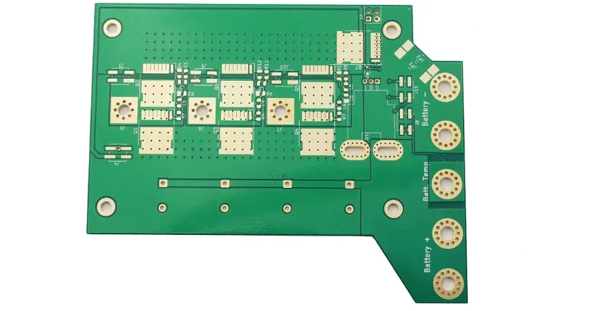
The 4 layer PCB represents a critical sweet spot in electronics design, offering a significant leap in performance over 2-layer boards without the cost and complexity of higher-count multilayer designs. This balance makes it the go-to choice for countless applications, from IoT devices to complex industrial controls. However, successful 4 layer PCB manufacturing is not a one-size-fits-all process. The technology you need depends entirely on your project's specific mechanical, electrical, and density requirements. This guide provides a clear, practical overview of the different manufacturing types, common stackups, core process steps, and essential design rules to help you get your board built right the first time.
1. Core Types of 4 Layer PCB Manufacturing
In real-world projects, 4 layer PCB manufacturing encompasses a range of specialized fabrication types. The one you select directly impacts the stackup, materials, design rules, cost, and ultimately, which PCB factory is the right partner for your needs.
Most engineers already understand the basics of multilayer design. The crucial step is mapping your application to the correct manufacturing mode to avoid over-engineering your board or failing to meet critical performance specifications.
Key 4 Layer PCB Manufacturing Modes
4 layer rigid PCB manufacturing
These are standard boards built on FR-4 PCB or high-Tg substrates. They feature a single lamination cycle, through-hole vias, and a classic signal–plane–plane–signal stackup, making them ideal for mainstream control, embedded, and mixed-signal designs where cost and robustness are paramount.4 layer flex PCB manufacturing
Utilizing polyimide-based constructions with thin copper and coverlay instead of solder mask, this type is used where the board must bend or fold inside compact devices. It's perfect for wearables, cameras, and sensors, and is a key strategy for eliminating cables and connectors. Explore our dedicated flex PCB manufacturing services for more detail.4 layer rigid-flex PCB manufacturing
These hybrid builds combine rigid FR-4 sections with integrated flexible tails in a single laminated structure. This enables 3D packaging and robust, vibration-resistant interconnects in applications like medical devices and compact embedded systems. Learn more about our rigid-flex PCB manufacturing capabilities.4 layer HDI PCB manufacturing
This high-density interconnect flow uses laser-drilled microvias, finer line/space rules, and often via-in-pad technology. It's chosen for breaking out fine-pitch BGAs or packing high-speed signals into a small footprint without increasing the layer count.4 layer high-speed and RF PCB manufacturing
This process is tuned for precise impedance control and low-loss materials. It involves carefully defined core and prepreg thicknesses and is aimed at USB 3.x, PCIe, Gigabit Ethernet, and other signal-integrity-sensitive designs. Check out our solutions for high-speed PCBs.4 layer power and high-current PCB manufacturing
These builds emphasize heavier copper, wide planes, dense thermal vias, and sometimes metal-backed structures. They are chosen for motor drives, LED lighting, and power supplies where current capacity and thermal management are the primary constraints. For extreme power needs, consider our heavy copper PCB options.
Matching Manufacturing Type to Your Project
For many products, standard rigid 4 layer PCB manufacturing offers the best price-to-performance ratio. However, as soon as your design demands miniaturization, flexible interconnects, high pin-count packages, or aggressive signal integrity and power density, you will need to step into the specialized realms of flex, rigid-flex, HDI, high-speed, or high-current fabrication. Choosing the right manufacturing mode early is the fastest way to avoid redesigns, schedule delays, and budget overruns.
2. Typical 4 Layer PCB Stackups by Application Type
Once you’ve selected your manufacturing type, you can define the stackup. Below are common configurations that 4 layer PCB manufacturers handle daily.
2.1 General-Purpose 4 Layer Rigid PCB Stackup
A classic stackup for digital control boards:
- L1: Signal
- L2: Solid Ground Plane
- L3: Power Plane (with some routing for slow signals)
- L4: Signal
Why it works:
- Each outer signal layer has an adjacent solid reference plane, which is excellent for EMI control.
- Provides good signal integrity for typical microcontroller and logic designs.
- Uses simple, low-cost materials and a single lamination cycle.
2.2 High-Speed 4 Layer Stackup (Impedance Controlled)
A common stackup for high-speed 4 layer PCB manufacturing:
- L1: High-Speed Signal
- L2: Ground Plane
- L3: Ground or Split Power/Ground Plane
- L4: High-Speed or Mixed Signal
Guidelines:
- Keep the L1–L2 spacing tight for microstrip impedance control.
- Use L2 and L3 as solid references; avoid cutting the reference plane under critical traces.
- Place differential pairs on a single outer layer where possible for easier impedance control.
Your manufacturer can help fine-tune trace widths and spacing based on their specific material set.
2.3 4 Layer Flex and Rigid-Flex Stackups
Common considerations for 4 layer flex PCB manufacturing:
- Use a thin polyimide core for the flex section with symmetrical copper on both sides.
- Create stiffer regions by adding localized FR-4 or polyimide stiffeners.
- Apply coverlay instead of solder mask over flexible areas.
For 4 layer rigid-flex PCB manufacturing:
- Rigid Region: A standard 4-layer FR-4 style stackup.
- Flex Region: A polyimide sub-stack integrated only where bending is required.
- Requires multiple bonding films and carefully designed transition zones from rigid to flex.
Stackup drawings must clearly define which layers exist in the rigid versus flex regions; otherwise, the fabricator cannot build the board correctly.
3. 4 Layer PCB Manufacturing Process Overview
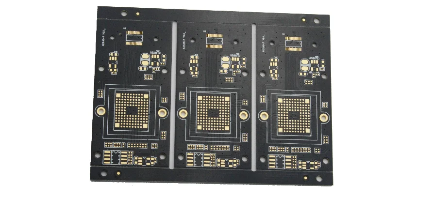
Regardless of the type, all 4 layer PCB manufacturing flows are built upon a few common stages.
3.1 Inner Layer Fabrication and Inspection
- Clean and prepare copper-clad cores.
- Apply photoresist, expose, and develop the inner layer images.
- Etch away unwanted copper to form inner traces and planes.
- Strip the resist and run Automated Optical Inspection (AOI) to catch shorts, opens, or pattern defects.
3.2 Lamination
- Stack the inner cores with prepreg and outer copper foils in a precise order.
- Press the stack under heat and pressure, causing the prepreg to flow and bond everything into a solid board.
- Cool the board under controlled conditions to prevent warpage and delamination.
3.3 Drilling and Via Metallization
- Perform CNC drilling (and laser drilling for microvias in HDI builds).
- Clean and condition the hole walls (desmear).
- Apply an electroless copper layer to seed the hole walls.
- Use electrolytic copper plating to build adequate thickness in the plated through-holes and on outer surfaces.
3.4 Outer Layer Imaging, Etching, and Surface Finish
- Apply photoresist to the outer layers, then expose and develop the pattern.
- Pattern plate and etch to create the final outer traces and pads.
- Apply solder mask and legend (silkscreen).
- Add a surface finish: HASL, lead-free HASL, ENIG, OSP, or others.
3.5 Testing, Profiling, and Final Inspection
- Conduct an electrical test (flying probe or fixture) for continuity and isolation.
- Perform mechanical routing or V-scoring to define the final board outline.
- Visually and automatically inspect for defects, contamination, or cosmetic issues.
- Complete final cleaning and vacuum packing.
At this point, the 4 layer PCB manufacturing is complete, and the boards are ready for assembly.
4. Design and DFM Tips for Different 4 Layer PCB Types
A major part of successful 4 layer PCB manufacturing is optimizing the design for the chosen process.
4.1 Rigid 4 Layer PCB Design Tips
- Adhere to your manufacturer’s minimum trace/space and annular ring rules.
- Place decoupling capacitors extremely close to the power pins of high-speed ICs.
- Avoid splitting ground planes or creating large cutouts under high-speed signals.
- Include clearly labeled test points to simplify debugging and production testing.
4.2 Flex and Rigid-Flex Design Guidelines
- Use curved trace routing in bend areas; avoid sharp 90-degree bends.
- Keep vias, pads, and other sharp copper features out of dynamic bend regions.
- Balance the copper distribution across flex layers to minimize curling.
- Clearly document bend areas, bend radii, and flex requirements in your fabrication notes.
4.3 HDI and High-Speed 4 Layer PCB Design Points
- Plan your BGA breakout strategy (e.g., microvia fan-out) early in the layout process.
- Keep via stubs as short as possible to maintain signal integrity.
- Maintain consistent differential pair geometry and length matching.
- Provide clear impedance targets and ensure reference planes are clean and continuous.
5. Cost and Lead Time Drivers in 4 Layer PCB Manufacturing
Not all 4 layer boards are priced equally. The final cost depends on:
- Board Size: How well your board fits on a standard production panel.
- Material Type: Standard FR-4 vs. high-Tg, low-loss, or polyimide materials.
- Copper Thickness: Heavier copper on each layer increases cost.
- Complexity: Flex and rigid-flex require more lamination cycles and manual handling.
- Tolerances: Finer trace/space rules and smaller drill sizes are more expensive.
- HDI Features: Microvias and via-in-pad technology add cost.
- Surface Finish: ENIG typically costs more than HASL or OSP.
Typical Lead Times:
- Standard 4 layer rigid PCBs: 5–10 working days for prototypes.
- HDI, flex, and rigid-flex: 10–20 working days, depending on complexity.
6. How to Choose the Right 4 Layer PCB Manufacturer
Because 4 layer PCB manufacturing spans so many technologies, no single factory excels at everything.
Key Evaluation Points:
- Do they publish clear capability tables for rigid, flex, and HDI manufacturing?
- Can they provide real stackup suggestions and impedance calculations?
- What quality certifications do they hold (ISO 9001, IATF 16949, etc.)?
- Do they support AOI, flying probe testing, and X-ray inspection?
- How responsive is their engineering team to DFM and stackup questions?
- Can they scale from prototypes to volume production?
For complex projects, prioritize a manufacturer's engineering support and process reliability over the absolute lowest quote.
7. FAQ About 4 Layer PCB Manufacturing
Q1: Which type of 4 layer PCB manufacturing should I choose for a compact, connector-free design? If you need to fold or wrap the board around mechanical structures, look at 4 layer flex or rigid-flex manufacturing. Rigid-flex is especially useful for eliminating connectors between several rigid sections while keeping everything in a single, reliable assembly.
Q2: Can I route high-speed signals on a standard 4 layer rigid PCB, or do I need HDI? Many high-speed interfaces can be successfully implemented on a standard 4 layer rigid PCB with a good stackup and controlled impedance. You typically only need 4 layer HDI PCB manufacturing when dealing with very fine-pitch BGAs, extremely tight routing density, or aggressive size constraints.
Q3: Is 4 layer flex PCB manufacturing always more expensive than rigid? Yes, 4 layer flex manufacturing is generally more expensive due to higher material costs, lower panel utilization, and more specialized processing. It should be chosen only when its flexing or 3D packaging capabilities provide clear benefits that justify the added cost.
Q4: How do I specify a stackup for 4 layer high-speed PCB manufacturing? Provide your target structure (e.g., signal–ground–power–signal), desired material type, and target impedance values (single-ended and differential). A capable 4 layer PCB manufacturer will respond with a detailed stackup proposal that includes exact material thicknesses and recommended trace geometries.
Q5: What files should I prepare for a 4 layer PCB manufacturing quote? At a minimum, you need Gerber or ODB++ files, NC drill files, a stackup drawing, and fabrication notes detailing materials, copper thickness, surface finish, and any impedance requirements. If you also need assembly, include a Bill of Materials (BOM) and pick-and-place files so your manufacturer can provide a full turnkey assembly quote.