
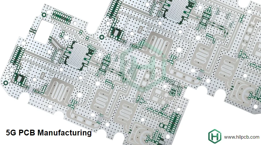
5G networks require PCB technology that can maintain signal integrity, minimize RF losses, and support dense electronic integration. Unlike conventional communication boards, 5G PCBs must operate across sub-6 GHz FR1 bands and millimeter-wave FR2 frequencies from 24 GHz to 100 GHz while handling high-speed digital processing, power amplification, and complex antenna systems.
A 5G PCB must address several engineering challenges simultaneously:
- Low dielectric loss at high frequencies
- Precise impedance control for RF signal paths
- Thermal management for high-power components
- High-density routing for massive MIMO antenna systems
- Reliable manufacturing consistency across production volumes
Advanced 5G PCB manufacturing combines specialized materials, HDI fabrication, controlled processes, and RF validation testing to meet the requirements of base stations, small cells, network equipment, and wireless devices.
What Sets 5G PCBs Apart from Other PCBs?
5G systems operate across multiple frequency ranges, creating different PCB requirements depending on the application. Sub-6 GHz systems focus on coverage, capacity, and antenna integration, while millimeter-wave systems require extremely precise RF performance.
Millimeter-Wave Circuit Challenges:
At frequencies above 24 GHz, minor manufacturing variations can significantly affect signal performance. Changes in trace width, copper roughness, dielectric thickness, and via geometry can create impedance discontinuities and increase insertion loss.
Traditional FR4 materials are generally unsuitable for demanding millimeter-wave RF circuits because their dielectric loss increases signal attenuation at higher frequencies. 5G RF designs typically require low-loss laminate materials with stable electrical properties. Our high-frequency PCB manufacturing process supports controlled impedance structures for high-frequency communication applications.
Massive MIMO Requirements:
5G base stations commonly use massive MIMO antenna arrays with dozens or hundreds of antenna elements. Some systems support configurations with up to 256 antenna elements.
These designs require PCBs that provide:
- Controlled impedance RF transmission lines
- Low crosstalk between antenna channels
- Efficient power delivery for RF amplifiers
- Effective thermal dissipation in compact layouts
- High layer-count routing capability
High-Speed Digital Interfaces:
5G infrastructure combines RF circuits with advanced digital processing hardware. Interfaces such as 100G Ethernet and DDR4/DDR5 memory require precise signal management.
PCB design must control:
- Differential pair impedance
- Trace length matching
- Return current paths
- Power distribution noise
- Signal timing margins
Integration Density:
Modern 5G equipment requires compact designs with increased functionality. HDI PCB technology enables smaller feature sizes through microvias, fine-line traces, and sequential lamination processes.
HDI structures allow engineers to:
- Reduce board size
- Increase routing density
- Improve signal integrity
- Support fine-pitch RF and processor components
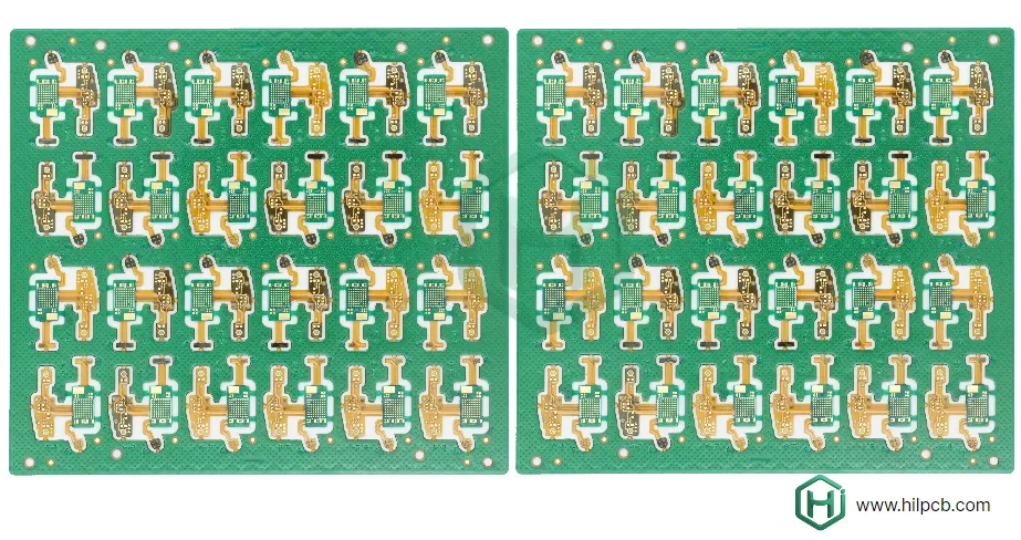
How to Achieve Low Loss and High Speed Signal Transmission
Maintaining signal quality at multi-gigabit data rates requires careful control of materials, manufacturing tolerances, and transmission structures.
Material Selection for Loss Minimization
At millimeter-wave frequencies, dielectric loss becomes a major contributor to signal attenuation. The dissipation factor (tan δ) of the PCB material directly affects insertion loss.
Standard FR4 materials may have tan δ values around 0.02 at 1 GHz, making them unsuitable for many 5G RF applications. Low-loss laminates with tan δ below 0.002 are commonly selected for high-frequency circuits.
Common 5G PCB materials include:
- Rogers RO4000 series: Provides a balance of RF performance, manufacturability, and cost efficiency with tan δ of 0.0027
- Rogers RO3000 series: Offers lower dielectric loss with tan δ values from 0.0010 to 0.0013 for demanding RF applications
- Polytetrafluoroethylene (PTFE) composites: Provides extremely low loss performance for advanced millimeter-wave designs
Material selection depends on operating frequency, loss budget, thermal requirements, mechanical constraints, and production volume.
For mixed RF and digital designs, engineers often use hybrid multilayer structures. Low-loss materials are applied to RF signal layers, while standard materials may be used for digital routing and mechanical layers. Our multilayer PCB manufacturing capability supports optimized stack-ups for complex 5G systems.
Controlled Impedance Across Frequency
5G RF circuits require tighter impedance control than many previous-generation wireless designs.
While lower-frequency applications may accept approximately ±10% impedance variation, millimeter-wave 5G circuits commonly require impedance control within ±5%.
Manufacturing control methods include:
- Electromagnetic simulation using frequency-dependent material models
- Laser direct imaging (LDI) with pattern resolution down to 10 μm
- Time-domain reflectometry (TDR) impedance verification
- Statistical process control maintaining dimensional tolerances to ±1 mil
These controls help maintain consistent RF performance between prototype builds and production quantities.
Via Design and Signal Transitions
Vias introduce parasitic inductance and capacitance that can affect RF performance. At millimeter-wave frequencies, conventional through-hole vias may create unwanted resonances caused by unused via stubs.
Common optimization methods include:
- Blind and buried vias: Reduce electrical length and improve routing density
- Via back-drilling: Removes unused via barrel sections that create signal reflections
- Ground via fencing: Creates RF isolation around sensitive transmission lines
- Coaxial via structures: Uses surrounding ground vias to maintain controlled impedance transitions
Proper via design is essential for maintaining signal integrity between PCB layers.
Surface Roughness Impact
Copper surface roughness affects high-frequency transmission because RF currents travel near the conductor surface due to the skin effect.
Standard electro-deposited copper with RMS roughness of approximately 3-5 μm can introduce additional insertion loss at 28 GHz, potentially adding 0.3-0.5 dB/inch.
To reduce conductor loss, high-frequency PCB manufacturers often specify:
- Reverse-treated copper foils
- Very low profile (VLP) copper
- RMS copper roughness below 1 μm
These materials reduce RF attenuation while maintaining reliable copper-to-laminate adhesion.
Differential Signaling
5G equipment uses high-speed differential interfaces for data transmission between processors, memory, and communication modules.
Key design requirements include:
- Controlled differential impedance, typically 85-100 ohms
- Trace length matching, typically within ±5 mils
- Consistent spacing between differential pairs
- Stable dielectric thickness across layers
Our high-speed PCB processes maintain these parameters through controlled stack-up design and manufacturing inspection.
Ensuring EMI/EMC Compliance for 5G PCBs
5G equipment operates in environments with significant electromagnetic activity. PCB designs must prevent unwanted emissions while protecting sensitive RF circuits from interference.
Key EMI/EMC control methods include:
- Shielding Strategies: Ground planes, RF compartments, and via fences reduce electromagnetic coupling between circuits.
- Power Distribution Network (PDN): Optimized power planes, decoupling capacitors, and controlled return paths reduce power noise.
- Common-Mode Filtering: Common-mode chokes and ferrite components reduce unwanted common-mode currents.
- Connector and Cable Interface Control: Filtered connectors and grounding structures prevent interference at external interfaces.
A properly designed 5G PCB maintains RF performance while meeting electromagnetic compatibility requirements.
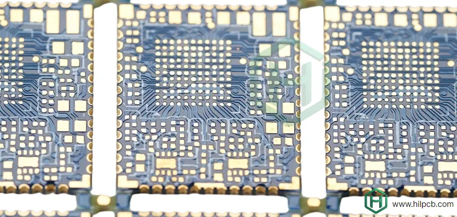
How We Ensure High Quality 5G PCB Manufacturing
5G PCB production requires tighter process control than standard electronic assemblies. Small dimensional variations can directly impact RF performance, especially at millimeter-wave frequencies.
Advanced Fabrication Technology
5G-capable PCB manufacturing uses specialized equipment and processes:
- Laser Direct Imaging (LDI): Provides trace width control with resolution down to 10 μm and improves registration accuracy.
- Sequential Lamination: Enables complex multilayer structures with buried vias and controlled impedance routing.
- Laser Drilling: Creates HDI microvias typically ranging from 75-100 μm in diameter.
- Automated Optical Inspection (AOI): Inspects inner and outer layers before lamination to identify defects early.
Material Handling and Storage
Low-loss RF laminates require controlled storage conditions because moisture absorption can change dielectric properties.
Materials are stored under controlled conditions:
- Relative humidity: 45-55%
- Temperature: 20-25°C
Material traceability includes documentation for:
- Dielectric constant
- Dissipation factor
- Laminate thickness
- Material lot information
This allows manufacturers to correlate electrical performance with material specifications.
Process Capability and Control
Critical manufacturing parameters are monitored through statistical process control (SPC), including:
- Copper thickness: ±5% tolerance
- Dielectric thickness: ±10%
- Layer registration: ±2 mil
- Via hole size: ±1 mil
Maintaining process capability indices (Cpk) above 1.67 for critical dimensions ensures stable production performance.
Electrical Testing
Every 5G PCB requires electrical verification before shipment.
Testing includes:
- Impedance Testing: TDR measurement confirms 50-ohm single-ended and 100-ohm differential impedance structures.
- Continuity and Isolation Testing: Confirms electrical connections and prevents unintended shorts.
- High-Potential Testing: Verifies dielectric insulation strength.
RF-critical boards may also undergo S-parameter testing using representative test coupons to validate:
- Insertion loss
- Return loss
- Crosstalk performance
Environmental Qualification
5G infrastructure equipment must operate reliably in demanding environments.
Qualification testing commonly includes:
- Thermal cycling from -40°C to +85°C
- 500 thermal cycles
- Microsection analysis
- Via reliability verification
- Solder joint inspection
These tests confirm long-term mechanical and electrical stability.
Best Materials for 5G PCBs
Material selection directly affects RF performance, thermal behavior, mechanical reliability, and manufacturing cost.
Rogers RO4000 Series
Rogers RO4000 laminates are widely used in 5G PCB applications because they combine RF performance with standard PCB manufacturing compatibility.
Key characteristics include:
- Dielectric constant (Dk): 3.38-3.48
- Dk tolerance: ±0.05
- Dissipation factor (tan δ): 0.0027 at 10 GHz
- Thermal conductivity: 0.62 W/mK
- Compatibility with standard FR4 processing equipment
RO4000 materials are suitable for many FR1 applications, including massive MIMO base stations operating below 6 GHz.
Our Rogers PCB manufacturing expertise supports optimized stack-up design and reliable production processing.
Rogers RO3000 Series
RO3000 materials are designed for applications requiring lower RF losses and improved temperature stability.
Key characteristics include:
- Ultra-low tan δ:
- RO3003: 0.0010
- RO3010: 0.0013
- Stable dielectric properties from -50°C to +150°C
- Strong mechanical reliability for harsh environments
RO3000 laminates are commonly used for millimeter-wave applications such as 28 GHz and 39 GHz 5G systems where reducing signal loss is critical.
PTFE-Based Composites
PTFE-based materials provide some of the lowest dielectric losses available for advanced RF circuits.
Typical advantages include:
- Dissipation factor below 0.0009
- Dielectric constants from 2.1 to 3.5
- Stable electrical performance up to 260°C
PTFE materials require specialized manufacturing processes, including controlled drilling, plating, and lamination methods.
Hybrid Material Constructions
Hybrid PCB structures combine different materials within one multilayer stack-up.
Typical configurations include:
- Low-loss laminates for RF layers
- FR4 materials for digital routing
- Dedicated power and thermal management layers
Hybrid construction reduces cost while maintaining RF performance where required.
Engineering considerations include:
- Thermal expansion matching
- Layer bonding reliability
- Via reliability during temperature cycling
- Prevention of delamination
Optimizing Delivery Times and Costs for 5G PCBs
5G PCB projects require both engineering precision and efficient production management.
Manufacturing optimization includes:
- Rapid Prototyping: Functional 5G prototypes in 5-10 working days, with expedited service available in 3-5 days for urgent development cycles.
- Design for Manufacturability (DFM): Early review of stack-up, impedance requirements, and via structures reduces prototype iterations by 30-50%.
- Scalable Production: Support for small batch assembly and large volume assembly maintains consistency from prototype builds to production.
- Cost Optimization: Panel utilization, material selection, and routing strategies are optimized to balance performance and manufacturing cost.
- Global Delivery and Support: Logistics support, compliance documentation, and engineering assistance simplify international production programs.
A controlled manufacturing approach reduces development risk while improving time-to-market.
Complete 5G Solutions from Design to Deployment
5G product development requires more than PCB fabrication. Successful deployment depends on integrated design support, assembly capability, RF validation, and production testing.
Our end-to-end 5G capabilities include:
- Advanced PCB fabrication for FR1 sub-6 GHz and FR2 millimeter-wave applications
- Precision SMT assembly for fine-pitch RF components and BGAs with 0.4mm pitch
- RF testing and characterization up to 110 GHz, including insertion loss, return loss, and isolation measurements
- Thermal simulation and management for high-density power amplifier designs
- EMI/EMC pre-compliance testing to reduce regulatory risk
- Complete turnkey assembly from bare PCB fabrication through programmed and tested electronic modules
A qualified 5G PCB manufacturing partner helps reduce design iterations, improve production reliability, and accelerate deployment of wireless infrastructure products.