
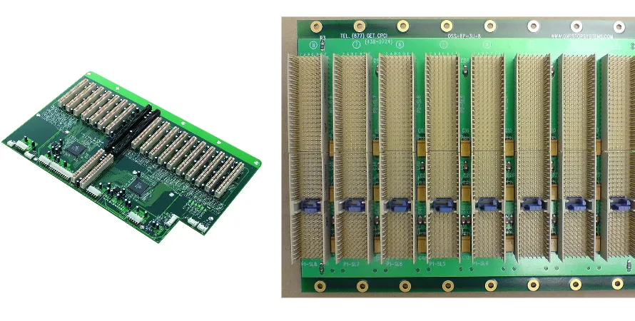
With exponential growth in artificial intelligence (AI) and machine learning (ML), data centers are undergoing an unprecedented architectural revolution. At the core of this revolution is the AI server—and the foundation of its performance is an electronic component that looks ordinary yet is extraordinarily complex: the AI server motherboard PCB. As a compliance and reliability engineer responsible for HALT/HASS, signal-integrity testing, and boundary scan, I know this backplane PCB is not only the physical platform connecting GPUs, CPUs, memory, and networking modules; it is also the “nervous system” that determines whether the entire system can run stably 24/7 under heavy load.
AI server backplane design and manufacturing have long moved beyond the scope of traditional server PCBs. The board must carry multi-kilowatt power, handle PCIe 5.0/6.0 (and even faster) signaling, and dissipate heat effectively inside a dense mechanical envelope. Any tiny design flaw or manufacturing defect can lead to signal distortion, power collapse, or thermal shutdown—causing catastrophic interruptions to data processing. From a reliability-engineering perspective, this article breaks down the core challenges and solutions for AI server backplane PCBs across high-speed signal integrity, power delivery, thermal management, and design-for-testability—so you can navigate this advanced technology with confidence.
Why is the AI server backplane PCB the nerve center of data flow?
Traditional server motherboards typically integrate the CPU, memory, and I/O on one board. AI servers, however, adopt a modular architecture to maximize parallel compute. They connect multiple GPU accelerator modules (such as NVIDIA’s SXM or OAM), CPU modules, high-speed network interface cards (NICs), and storage devices through a high-density, high-performance backplane. This architecture makes the AI server motherboard PCB the communication backbone of the entire system.
Its central role shows up in several ways:
- Ultra-high-bandwidth interconnect: AI model training requires frequent exchange of massive data sets across GPU clusters. The backplane PCB must provide ultra-low-latency, ultra-high-bandwidth physical links for GPU-to-GPU communication (e.g., NVLink) and CPU-to-GPU communication (e.g., PCIe). This demands exceptional high-speed transmission capability, making it a classic high-speed AI server motherboard PCB application scenario.
- Massive power distribution: A single AI accelerator can consume 700 W—or even more than 1000 W—and a fully populated AI server can draw several kilowatts. The backplane PCB must distribute these huge currents precisely and stably to each compute module, placing extreme demands on power distribution network (PDN) design.
- Complex system topology: To enable flexible expansion and upgrades, AI server backplanes may support complex connection topologies such as All-to-All, Ring, or hybrid architectures. This drives extremely high routing density, often with more than 20 layers—making both design and manufacturing highly challenging.
- Reliability and serviceability: As a core data-center asset, AI servers require extremely high operational reliability. Backplane design must consider long-term stability and fast diagnostics/replacement when failures occur—critical throughout the product lifecycle, especially during NPI EVT/DVT/PVT phases (engineering, design, and production validation tests for new product introduction).
High-speed signal integrity: mastering PCIe 5.0/6.0 design challenges
With the widespread adoption of PCIe 5.0 (32 GT/s) and the arrival of PCIe 6.0 (64 GT/s), AI server backplane signal rates have entered the RF domain. At these speeds, PCB traces are no longer simple “wires”—they behave as complex transmission-line systems. As reliability engineers, ensuring Signal Integrity (SI) becomes a top priority.
Key challenges include:
- Insertion loss: High-speed signals attenuate during transmission, especially across long backplane routes and multiple connectors. We must select Ultra-Low Loss or Extremely-Low Loss PCB materials—such as Megtron 6 or Tachyon 100G—to reduce dielectric loss (Df) and conductor loss.
- Impedance control: Differential-pair impedance must be tightly controlled at 100 Ω or 85 Ω (within ±5%). Any discontinuity—vias, connectors, or width changes—creates reflections, collapses the eye diagram, and increases bit error rate. Precise impedance control is a core capability of high-speed pcb manufacturing.
- Crosstalk: In high-density routing, electromagnetic coupling between adjacent signal lines causes interference. We suppress far-end crosstalk (FEXT) and near-end crosstalk (NEXT) by optimizing spacing, planning routing paths, and using ground shielding layers.
- Timing & jitter: Jitter compresses the horizontal eye opening and impacts sampling margin. From material selection to via design, every step must focus on minimizing jitter sources.
Throughout the NPI EVT/DVT/PVT process, we use simulation tools such as ANSYS HFSS and Keysight ADS for extensive pre-layout SI simulation and post-layout verification, ensuring the design meets specification requirements before it goes into fabrication.
PCB loss-budget comparison across PCIe generations
| PCIe generation | Data rate (GT/s) | Nyquist frequency (GHz) | Total channel loss budget (dB) | PCB material requirement |
|---|---|---|---|---|
| PCIe 4.0 | 16 | 8 | ~28 | Mid-loss / Low-loss |
| PCIe 5.0 | 32 | 16 | ~36 | Low-loss / Ultra-low-loss |
| PCIe 6.0 | 64 (PAM4) | 16 | ~32 | Ultra-low-loss / Extremely-low-loss |
How do complex stack-ups and via technologies impact backplane performance?
A high-performance AI server motherboard PCB typically has 20 to 30+ layers. Its stack-up is the foundation of the entire project: a well-designed stack-up not only provides sufficient routing resources, but also enables impedance control, crosstalk shielding, and ultra-low-impedance power networks.
Our stack-up design principles include:
- Symmetric construction: To prevent bow/warp during manufacturing, the stack-up must be symmetric—especially critical for very large backplanes.
- Reference-plane integrity: Every high-speed signal layer must sit adjacent to a solid GND or PWR plane as its return-path reference. Any split in the reference plane can create impedance discontinuities and severe EMI issues.
- Power/ground plane pairing: Tight coupling between PWR and GND planes forms natural plane capacitance, providing a low-impedance path for high-frequency currents and improving power integrity (PI).
Vias connect traces between layers, but for high-speed signals they can also become a major bottleneck. Conventional through-hole vias create unwanted stubs that radiate like antennas at high frequency and cause severe reflections. To mitigate this, we use advanced via technologies:
- Back-drilling: After fabrication, the extra via stub is drilled out from the backside. This is a cost-effective way to improve SI and is nearly mandatory for PCIe 4.0 and above.
- HDI (High-Density Interconnect): Using laser-drilled microvias as well as blind and buried vias. This dramatically increases routing density and shortens signal paths, reducing parasitic inductance and capacitance. Highleap PCB Factory (HILPCB) has extensive experience with HDI PCB manufacturing to support complex design needs.
Power integrity (PDN) is critical for high-power AI modules
If signal integrity ensures data is transmitted “clearly,” then Power Integrity (PI) ensures the system runs “strong.” AI accelerators demand extremely high transient current (di/dt)—huge current in a very short time. If PDN design is weak, voltage rails can droop and trigger immediate system crashes.
Our PDN strategy focuses on ultra-low impedance across the entire path from the VRM (voltage regulator module) to the GPU/CPU:
- Plane capacitance: Use tightly coupled power and ground planes to create large-area plane capacitance, providing a low-impedance path for high-frequency noise.
- Decoupling capacitors: Place many decoupling capacitors close to chip power pins. They act like local energy reservoirs that respond quickly to transient load steps. Capacitor selection and placement should cover the full spectrum from low frequency to high frequency.
- VRM placement and copper design: Place VRMs as close as possible to the load (GPU/CPU) to shorten current paths. Use wide/thick copper pours or heavy copper pcb technology to reduce DC IR drop and resistive loss.
A robust PDN design requires reliability on par with automotive-grade AI server motherboard PCB expectations, because any power fluctuation can cause compute errors—unacceptable for mission-critical applications such as scientific computing or financial modeling.
⚡ PDN integrity: power distribution network design matrix
End-to-end stability control—from DC IR drop to AC impedance
Design guideline: Reject rules of thumb. Use the chip’s transient current $\Delta I$ and allowable voltage ripple $\Delta V$ to calculate the full-band target impedance $Z_{target}$. Keep the PDN impedance curve below the target across the chip’s operating bandwidth to prevent systemic voltage droop.
Placement strategy: Build a hierarchical energy-storage system. Bulk capacitors cover low-frequency compensation; small decoupling capacitors cover high-frequency transients. Physical location determines effectiveness: small 01005/0201 capacitors must sit right at the power pins to minimize parasitic inductance (ESL).
Engineering point: Use plenty of vias in the power/ground network. Never let multiple decoupling capacitors share a single via—common-path inductance can couple noise. Use a symmetric ground-via pattern to reduce loop inductance in high-frequency return paths.
Closed-loop verification: Run DC IR-drop and AC impedance simulations before tape-out. Use current-density heat maps to identify “neck-down” or bottleneck regions in power planes, eliminate local overheating risks, and optimize plane splitting.
For high-speed digital systems below 1 V, HILPCB offers Embedded Capacitance material solutions that significantly reduce high-frequency impedance. Meanwhile, our high-precision Heavy Copper Layering processes ensure extremely low IR-drop loss in your DC power network.
Thermal management: cooling multi-kilowatt AI servers
Heat is the number-one killer of electronics reliability. A fully loaded AI server chassis can consume 10–15 kW, with heat flux far beyond traditional servers. While the AI server motherboard PCB itself is not the primary heat source, it carries all high-power devices and becomes a key heat-transfer path.
Our thermal management strategy is systemic, and PCB design is a critical part of it:
- High-thermal-conductivity materials: Select PCB laminates with high glass-transition temperature (Tg) and higher thermal conductivity (Tc), such as high-Tg FR-4 or more advanced ceramic-filled materials, to keep mechanical and electrical performance stable at elevated temperature.
- Optimized copper distribution: Use large copper areas on outer and inner layers, using copper’s high thermal conductivity to move heat away from sources (such as VRMs and chip underfills) toward heatsinks and chassis structures.
- Thermal vias: Place dense arrays of thermal vias under hot components to conduct heat vertically to the opposite side of the PCB or to internal heat-spreading planes, significantly reducing thermal resistance.
- Embedded thermal solutions: For extremely high-power regions, use advanced options such as embedded copper coins or heat pipes, integrating the thermal structure inside the PCB for the most efficient conduction path.
Effective thermal management not only prevents throttling or damage from overheating, but also extends the entire system’s lifetime—forming the foundation of long-term reliability.
Reliability validation in manufacturing and assembly: from NPI to mass production
A perfect design that cannot be manufactured precisely is only theory. For products as complex as AI server motherboard PCB, collaboration between design and manufacturing (DFM/DFA) is essential. At specialist manufacturers like HILPCB, we engage early and provide DFM analysis to ensure that a design meets performance targets while also enabling high-yield mass production.
The product lifecycle follows a strict NPI EVT/DVT/PVT process:
- EVT (Engineering Validation Test): This phase validates basic functionality and design concepts. A small number of prototype boards—i.e., AI server motherboard PCB low volume builds—are produced for electrical functional verification, initial SI measurement, and basic firmware bring-up.
- DVT (Design Validation Test): The most comprehensive phase. We perform full SI/PI/thermal/EMC testing. We also run HALT (Highly Accelerated Life Testing) by applying stresses far beyond spec (temperature and vibration) to rapidly expose weak points in design and manufacturing.
- PVT (Production Validation Test): This phase validates mass-production stability and yield. We run a pilot build using final production tooling and test programs to ensure every step—from fabrication to assembly—is stable and repeatable.
Through these rigorous validations, we ensure every delivered high-speed AI server motherboard PCB can operate long-term at the customer site without failures.
🚀 AI server backplane: digital NPI ramp-up and quality engineering
A system-level verification flow for multi-GPU interconnects, high-speed cable backplanes, and 10 kW+ power architectures
Based on 224G path planning, run coordinated full-wave SI/PI/Thermal simulation and define Ultra-Low Loss material specs.
Engineering prototype validation, focusing on power-up sequencing, interface logic, and mechanical fit for the backplane (orthogonal) connector.
Comprehensive reliability testing. Introduce HALT (Highly Accelerated Life Testing) to validate eye-opening margin and gold-finger wear under extreme vibration and high-heat conditions.
Lock down mass-production processes. Use Run@Rate to validate back-drill tolerance, lamination accuracy, and impedance CPK stability for large backplanes above 20 layers.
Move into sustained delivery. Run HASS (Highly Accelerated Stress Screening) and use automated test equipment (ATE) to ensure electrical consistency across every shipped backplane.
For high-aspect-ratio backplanes with 20+ layers, we provide an ASL (Adaptive Scaling Logic) compensation algorithm during NPI. By modeling inner-layer material shrinkage, we improve via registration accuracy in high-frequency regions by 30%, helping your AI program transition smoothly from prototype to SOP.
Boundary-Scan/JTAG in complex backplane testing
As BGA (ball grid array) packages continue to increase pin density, traditional ICT (in-circuit test) methods—flying probes or bed-of-nails fixtures—can no longer access most solder joints. This creates major challenges for PCBA (printed circuit board assembly) quality verification. In this context, Boundary-Scan/JTAG (IEEE 1149.1) becomes essential.
Boundary-Scan/JTAG is a test architecture built into many modern ICs (such as CPUs, FPGAs, and ASICs). It adds a “boundary-scan cell” at each IC pin and chains them into a scan path. Through the JTAG Test Access Port (TAP), we can:
- Test connectivity: Detect opens, shorts, and solder defects between BGA pins without physical probes—critical when validating thousands of connections between the backplane and daughter-card connectors.
- In-system programming: Program and configure FPGAs, CPLDs, flash, and other devices on-board, simplifying production flow.
- Assist functional testing: During early power-up, JTAG is a powerful tool for board-level debugging and diagnosis, helping engineers pinpoint hardware issues quickly.
For AI server backplane assembly test, integrating Boundary-Scan/JTAG is a must. It covers test blind spots that ICT cannot reach, improves throughput, and enables more accurate failure localization—providing key assurance for complex, high-density PCBA quality.
How to choose the right AI server backplane PCB manufacturer
Choosing the right manufacturing partner is critical to an AI server program’s success. A strong manufacturer is not just a build-to-print supplier; it should provide deep technical support, supply-chain stability, and robust reliability assurance.
When evaluating a manufacturer, focus on these core capabilities:
Technical capability:
- High layer count and large size: Can they stably produce 30+ layer PCBs larger than 600 mm × 800 mm?
- Advanced material experience: Do they have proven experience processing high-speed materials such as Megtron 6/7 and Tachyon 100G?
- Precision manufacturing tolerance: Can they meet strict trace width/spacing control (e.g., 3/3 mil), precise impedance control (±5%), and high-accuracy back-drill depth control?
- Advanced process support: Do they support advanced builds such as HDI, embedded passive/active components, and heavy copper?
Quality and reliability system:
- Certifications: Are they certified to ISO 9001, ISO 14001, IATF 16949, etc.? Even if the product is not automotive, an automotive-grade AI server motherboard PCB quality control mindset demonstrates a commitment to high reliability.
- Test capability: Do they have advanced AOI/AVI and X-ray inspection, and can they support Boundary-Scan/JTAG testing?
- Reliability lab: Can they perform environmental reliability tests such as thermal shock, temperature-humidity cycling, and vibration?
Service and support:
- One-stop service: Can they offer turnkey assembly from PCB fabrication to component sourcing, SMT, and final assembly to simplify supply-chain management?
- DFM/DFA support: Do they provide early-stage engineering support to optimize design, reduce cost, and improve manufacturability?
- Flexible capacity: Can they support fast prototypes and AI server motherboard PCB low volume builds, while also scaling to mass production when needed?
Highleap PCB Factory (HILPCB) focuses on high-layer-count, high-density, high-reliability PCB fabrication and assembly. With extensive program experience in high-speed AI server motherboard PCB, we offer one-stop solutions from design optimization to final delivery.
FAQ
Why is the AI server backplane PCB such a critical board in the system?
Because it is the interconnect backbone linking GPUs, CPUs, memory, NICs, and storage modules. Its quality directly affects bandwidth, power delivery, uptime, and serviceability across the whole server.
What makes PCIe 5.0 and PCIe 6.0 routing so difficult on AI server backplanes?
At those data rates, insertion loss, impedance discontinuities, crosstalk, and jitter all become major channel risks. That forces careful material selection, simulation, connector planning, and via optimization.
Why must power integrity and thermal design be treated together?
Multi-kilowatt AI systems create both heavy current demand and concentrated heat. A backplane that cannot maintain a low-impedance PDN and an effective cooling strategy will face voltage droop, hot spots, and stability problems.
Why is Boundary-Scan/JTAG still valuable on complex AI backplanes?
It helps test hidden interconnects around dense BGA devices, supports in-system programming, and speeds up hardware fault isolation. That makes it especially useful when ICT access is limited.
Conclusion
AI server motherboard PCB is one of the most technically dense and challenging components in modern AI infrastructure. It brings together advanced high-speed digital design, RF effects, power electronics, and thermodynamics. As reliability engineers, we know that building a stable, high-performance AI server backplane requires relentless attention to detail at every stage of design, manufacturing, and test.
From selecting the right ultra-low-loss materials, to designing a robust PDN and effective thermal strategy; from optimizing signal paths with back-drilling and HDI, to rigorous validation throughout NPI EVT/DVT/PVT; and finally, ensuring assembly quality with advanced techniques like Boundary-Scan/JTAG—every decision directly impacts end-product performance and reliability.
Handling these challenges requires deep expertise and strong manufacturing capability. Partnering with an experienced, technology-leading provider like HILPCB can be the difference-maker for your next-generation AI server program. If you are developing next-generation AI servers and need a reliable PCB fabrication and assembly partner, contact us today—our engineering team can provide a free DFM review and a competitive quote for your project.