
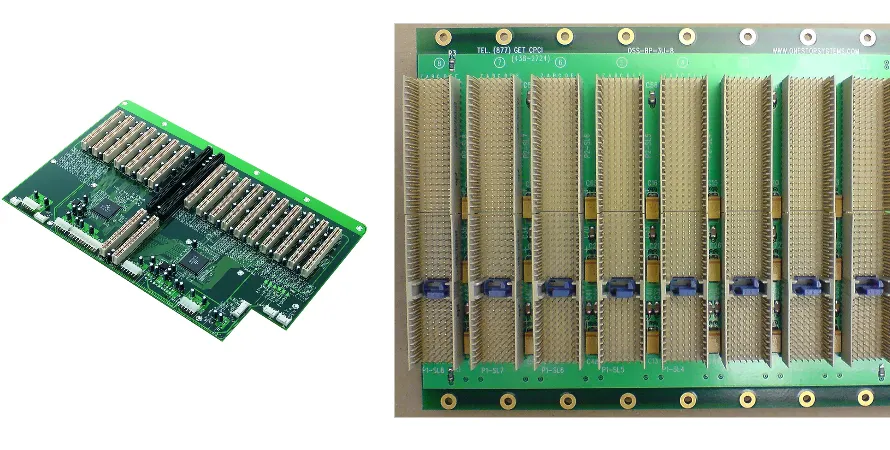
With the explosive growth of generative AI and LLM workloads, AI servers are demanding compute at an unprecedented pace. As the core platform carrying GPU, CPU, HBM, and high-speed interconnect modules, AI server motherboards and their backplane (Backplane) PCB face tougher-than-ever design and manufacturing constraints. A tiny design miss or manufacturing defect can become a system-level bottleneck—or a failure. That’s why a complete, rigorous AI server motherboard PCB checklist is essential.
This checklist is more than a set of design rules. It’s a system engineering guide that connects the full lifecycle from concept to mass production, spanning material selection, Signal Integrity (SI), Power Integrity (PI), thermal management, DFM, and DFT. As a detailed AI server motherboard PCB guide, this article breaks down the checklist’s key items to help engineers and program managers tame complex high-speed interconnect designs and deliver high-performance, high-reliability AI server hardware. Working with an experienced manufacturer like Highleap PCB Factory (HILPCB) helps maximize the value of the checklist and ensure your design lands as intended.
Why backplane stackup design is the foundation of success
In AI servers, the backplane PCB is not just mechanical support—it’s the electrical backbone interconnecting compute, storage, and network cards. Its stackup (Stack-up) directly determines electrical performance, reliability, and manufacturing cost, and it is the starting point for all downstream design work.
An optimized stackup must consider:
Material selection: AI servers often run at PCIe 5.0 (32GT/s), PCIe 6.0 (64GT/s), and beyond, where attenuation becomes a dominant challenge. You typically need Ultra-Low Loss or Extremely-Low Loss laminates such as Megtron 6/7 or Tachyon 100G. Building a qualified low-loss AI server motherboard PCB is step one for meeting high-speed channel targets.
Impedance control: High-speed differential pairs (PCIe, CXL, NVLink) demand tight impedance targets—commonly 85Ω, 90Ω, or 100Ω—with tolerance often within ±5%. Stackup design sets the impedance baseline via dielectric thickness, copper thickness, and trace geometry.
Reference plane integrity: High-speed signals need continuous, unbroken reference planes (GND or PWR) to provide clean return paths and suppress crosstalk and EMI. Signal layers should be adjacent to solid reference planes and avoid crossing splits.
Layer count & symmetry: AI backplanes often exceed 20 layers and may reach 40+ layers. Symmetry is critical to prevent warpage driven by thermal stress in fabrication and assembly.
How to manage SI for PCIe Gen5/Gen6 and CXL
SI is the core of AI backplane design. At 64GT/s, even small distortions can drive BER up dramatically and threaten system stability.
Differential pair routing: Follow strict length matching and tight coupling. Length match tolerance is often kept within 1–2mil to reduce skew. Avoid 90° corners; use arcs or 45° routing to reduce impedance discontinuities.
Loss budget management: Total insertion loss from CPU/GPU die to add-in card die is limited. You must quantify loss from PCB traces, vias, connectors, and more—and keep the total within spec. That typically requires early channel simulation, selecting appropriate low-loss AI server motherboard PCB materials, and optimizing routing strategies.
Crosstalk suppression: High-density routing makes crosstalk a primary challenge. Increase pair-to-pair spacing (often >3–5× trace width), use GND plane isolation, and use orthogonal routing between adjacent stripline signal layers to reduce NEXT and FEXT. For complex High-Speed PCB, detailed SI analysis is mandatory.
Vias and connector transitions: SI bottlenecks you can’t ignore
In multilayer PCB, vias are required to connect layers—but they’re also one of the biggest sources of impedance discontinuity in high-speed channels.
Via stubs (Stub): With Through-hole Via, when a signal transitions from the top layer to an inner layer, the unused lower portion becomes a stub that can resonate at high frequency and seriously degrade SI. For >10Gbps signals, Back-drilling is often required to remove unused stubs precisely.
Via optimization: Optimizing pad and anti-pad dimensions improves impedance matching. Adding Stitching Vias next to differential vias provides better return paths and reduces noise.
Connector footprint design: High-density connectors (e.g., MCIO, Gen-Z) have extremely dense BGA/SMT pad fields where routing is tight and SI risk concentrates. Use 3D EM simulation to model and optimize the connector region and ensure a smooth transition from PCB traces to connector pins.
🖥️ AI server backplane PCB full lifecycle flow
A closed-loop manufacturing system for high-compute backplanes—integrating ultra-multi-layer design, high-frequency materials, and end-to-end simulation validation.
Confirm PCIe 5.0/6.0, high-speed bus protocols, and channel density; define mechanical dimensions for the backplane.
Choose Ultra-Low Loss laminates and design a symmetric stackup to control warpage and optimize impedance.
Run SI, PI, and thermal simulations to estimate eye performance and temperature rise.
High-density routing, Backdrill planning, and Via-in-Pad processes to deliver high-performance interconnect.
Manufacturability analysis and test coverage evaluation for ultra-thick boards (over 4.0mm) and high-aspect-ratio vias.
Precision lamination for high-layer-count backplanes, validated by flying probe and TDR impedance tests.
Enable MES traceability and complete large-connector press-fit plus system integration tests.
How to build a stable and efficient PDN
A single AI accelerator (GPU) can exceed 1000W peak power and draw hundreds of amps. Delivering stable, clean power to these “power hungry” loads is the primary job of the PDN.
Low-impedance PDN design: The PDN target is extremely low impedance across a wide band (DC to GHz) to handle load transient current. This is achieved with large-area power/GND planes, sufficient decoupling capacitors, and optimized VRM placement.
Decoupling strategy: Mix capacitance values and packages. Large electrolytic/tantalum capacitors act as “reservoirs” for low-frequency high current, while many small MLCC close to chip power pins filter high-frequency noise.
IR Drop analysis: Under high current, copper resistance causes notable IR Drop. Use PI tools to ensure VRM-to-chip drop stays within limits (often 2–3%). Options include widening power paths, adding power layers, or using Heavy Copper PCB in critical regions.
Thermal management: keeping AI servers stable
High power and heat are inseparable. High-power devices on AI motherboards/backplanes (GPU, CPU, VRM, high-speed transceivers) generate massive heat; without proper dissipation, throttling, performance loss, and even permanent damage can occur.
Electro-thermal co-simulation: Modern flows emphasize co-simulation. Joule heating from current in copper, and temperature-driven changes to Dk and Df, must be considered together in a closed loop.
PCB-level thermal solutions:
- Thermal Vias: dense thermal via arrays under hot components to conduct heat to heatsinks/chassis through the PCB.
- Copper Pour: large copper pours on outer and inner layers to spread heat laterally.
- High thermal conductivity materials: choose laminates with higher thermal conductivity (Tc) and high Tg to maintain mechanical and electrical stability at temperature.
This AI server motherboard PCB guide highlights that thermal design and electrical design must be done in parallel—neither can be missing.
High-speed PCB material comparison
| Material grade | Dk (@10GHz) | Df (@10GHz) | Tg (°C) | Typical use |
|---|---|---|---|---|
| Standard FR-4 | ~4.5 | ~0.020 | 130-140 | Low-speed control boards |
| Mid-loss (Mid-Loss) | ~3.8 | ~0.010 | 170-180 | PCIe Gen3/4 server motherboards |
| Low-loss (Low-Loss) | ~3.5 | ~0.005 | >180 | PCIe Gen5, 100G Ethernet |
| Ultra-low loss (Ultra-Low Loss) | ~3.2 | <0.003 | >200 | PCIe Gen6/7, 400G+ networking, AI server backplanes |
DFM and DFT: the bridge from design to mass production
If a design looks perfect in simulation but cannot be manufactured and tested economically and reliably, it fails. DFM and DFT bridge theory and reality.
DFM: In design, you must account for fab capabilities: min line/space, min drill size, via aspect ratio, BGA pad design, and more. Early alignment with the PCB manufacturer (e.g., HILPCB) avoids expensive late changes.
DFT: AI server boards have extreme component density; many critical joints (e.g., BGA) cannot be inspected visually or by conventional probes.
- Boundary-Scan/JTAG: A crucial test method. With TAP integrated in ICs, you can detect opens/shorts on BGA pins without physical probes. Planning the JTAG chain at design time is a baseline DFT requirement.
- Test points & fixtures: For key analog signals and power rails, reserve test points. Plan Fixture design (ICT/FCT) early so probes can reliably contact points without damaging the board.
How manufacturing processes determine final performance
Great design requires top-tier manufacturing to realize. For AI server Backplane PCB, the following processes directly affect results:
- Impedance control accuracy: Advanced etch compensation and lamination control are needed to keep tolerance within ±5%.
- Drilling accuracy: Precision mechanical drilling and laser drilling (for HDI microvias) enable dense interconnect and reliable vias. Backdrill depth accuracy is equally critical.
- Surface finish: For high-frequency signals and fine-pitch BGA, ENIG or ENEPIG is commonly used to provide flat pads and strong solderability while reducing high-frequency skin-effect impact.
Choosing an experienced, well-equipped manufacturer like HILPCB is key to successfully producing a complex low-loss AI server motherboard PCB to spec.
HILPCB AI server backplane manufacturing capability
Max layer count
60+
Min line/space
2/2 mil
Impedance control
±5%
Max board thickness
10mm
Supported materials
Megtron 6/7, Tachyon 100G, Rogers
Advanced processes
Backdrill, HDI, embedded resistor/capacitor
Assembly and test: the last gate to validate the design
After fabrication, high-quality SMT Assembly and strict testing are the final guarantees of product functionality.
- SMT challenges: AI server motherboards typically include very large BGAs (CPU/GPU) and thousands of fine-pitch parts. This requires accurate solder paste printing, high-precision placement, and optimized reflow profiles to avoid opens, bridging, or component damage.
- Inspection methods: AOI checks general placement quality, while 3D X-ray (AXI) is the gold standard for BGA joints—finding internal defects invisible to the eye and AOI.
- Functional test (FCT): After assembly, run FCT to validate the board meets design intent. A well-designed Fixture design (ICT/FCT) is critical to emulate real conditions and stress-test high-speed interfaces and power systems. Boundary-Scan/JTAG is also commonly executed as an effective complement to FCT to locate faults quickly.
Reliability and protection: ensuring long-term stability
AI servers commonly run 24/7 in data centers, with extremely high reliability requirements.
- IPC standards: Design and manufacturing should follow high-reliability standards such as IPC-6012 Class 3 or Class 3A, which set tighter requirements on conductor width, annular ring, dielectric thickness, and more.
- Environmental robustness: Data center environments may involve dust and humidity variation. To improve long-term PCBA reliability, Conformal coating is an effective protection method. It applies a thin, uniform protective film that helps block moisture, dust, and chemical corrosion.
- Applying Conformal coating can significantly reduce short/corrosion risk caused by environmental factors and is an important reliability upgrade for AI servers deployed across diverse environments.
Conclusion
Building a successful AI server motherboard or backplane is complex system engineering—far beyond “just connecting circuits.” You need a clear, comprehensive AI server motherboard PCB checklist from day one, covering architecture, materials, SI/PI/thermal simulation, DFM/DFT planning, and close collaboration with fabrication and assembly partners.
As shown above, decisions like selecting low-loss AI server motherboard PCB materials, implementing Boundary-Scan/JTAG, planning Fixture design (ICT/FCT), and applying Conformal coating all have deep impact on performance and reliability.
To meet these challenges, you need a partner who not only understands your intent but can also provide professional fabrication and assembly recommendations. With deep experience in high-speed and high-density PCB, HILPCB offers one-stop service from DFM review and prototyping to volume production and assembly—helping turn leading-edge AI designs into reliable, high-performance products.
Common Questions
Why does an AI server motherboard or backplane need a formal checklist?
Because these boards combine high layer count, dense BGAs, high-speed links, power delivery, thermal constraints, manufacturability, and test access. A checklist keeps critical decisions aligned before layout and helps prevent expensive late-stage rework.
Why should material selection and SI/PI/thermal simulation be decided early?
Because stackup, loss budget, PDN behavior, and cooling strategy directly affect routing feasibility and reliability. If those decisions are delayed, the board may pass an early review but still fail signal, power, or thermal targets later.
Why are DFM, DFT, and assembly planning part of the checklist?
Because a board that is difficult to fabricate, inspect, or test will create yield, schedule, and field-reliability problems. Early planning for drill rules, impedance control, JTAG, test points, fixtures, and SMT constraints reduces those risks.
Why do protection and reliability measures matter so much for AI servers?
Because AI servers run continuously with high power density in demanding data center conditions. Standards compliance, coating, thermal margin, and process control help prevent drift, corrosion, premature failure, and unstable long-term operation.