
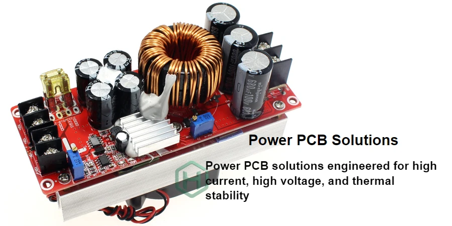
- An energy management PCB should be reviewed as a measurement and control board that also carries real power and isolation risk, not just as a low-voltage logic board.
- The first checks are current and voltage sensing topology, isolation boundaries, power-conversion heat flow, communication interfaces, and EMC exposure.
- Most design failures show up as inaccurate measurement, noisy control behavior, weak surge margin, thermal instability, or poor isolation implementation.
- The board architecture should separate metrology, power, communication, and service interfaces early so layout and compliance reviews are still cheap to fix.
- A stable release path usually needs fabrication, assembly, test, and regulatory expectations aligned before prototype spin.
An energy management PCB is the control and measurement board used in products such as smart meters, battery systems, solar controllers, energy gateways, and distribution monitors. It usually needs careful review of sensing accuracy, isolation strategy, power-stage layout, EMC behavior, and manufacturability because the finished product has to measure reliably while handling real electrical stress in the field.
Contents
- What to review first on an energy management PCB
- Key design and manufacturing rule table
- Early engineering risk table
- How sensing, isolation, and routing interact
- How power conversion, heat, and EMC should be reviewed
- What prototype and manufacturing teams should lock down before release
- FAQ
- Next steps
- References
- Author and review
What to review first on an energy management PCB
An energy management PCB often combines measurement, control, communication, and power handling on one platform. That mix is what makes these boards tricky. A design can appear electrically complete and still fail because the sensing path is too noisy, the isolation strategy is only schematic-deep, or the power section heats the metrology section until readings drift.The first review points are usually:
- which current and voltage sensing method the board uses and how noise, offset, and layout parasitics affect accuracy
- where hazardous or higher-energy domains begin and how the isolation boundary is physically maintained on the board
- whether the power stage, converter, relays, drivers, or protection devices create heat or switching noise that can corrupt measurement
- whether communication sections such as RS-485, CAN, Ethernet, or wireless modules are separated well enough from sensitive analog areas
- how the product will be tested for electrical safety, EMC, calibration, and assembly quality before pilot release
For boards that combine control logic with significant current or thermal loading, it is often useful to review the structure against heavy copper PCB and high Tg PCB options before layout freeze.
Key design and manufacturing rule table
| Rule / parameter | What to check first | Why it matters | How to verify | If ignored | | --- | --- | --- | --- | --- | | Sensing architecture | Confirm whether shunt, transformer, hall, or isolated sensing fits the product target | Accuracy, bandwidth, isolation, and cost all depend on sensing choice | Schematic review, calibration plan, error-budget review | Drift, inaccurate readings, redesign late in NPI | | Isolation boundary | Separate hazardous, power, sensing, and logic domains physically and visibly | Safety performance depends on real spacing, barriers, and layout discipline | Creepage review, enclosure review, [Gerber viewer](/tools/gerber-viewer/) inspection | Failed safety review or expensive board rework | | Power-stage zoning | Keep switching converters and high-current paths away from sensitive measurement nodes | Switching noise and thermal coupling can corrupt measurement | Placement review, return-path review, thermal review | Noise, false alarms, unstable metrology | | Communication interface layout | Protect bus and I/O sections from surge, ESD, and ground mismatch | Field reliability often depends on interface robustness | TVS review, connector review, EMC pre-review | Communication faults and field returns | | Thermal margin | Review shunts, regulators, relays, and power devices as one heat system | Metering and control accuracy can move with temperature | Thermal simulation, copper review, powered prototype test | Drift, derating, local overheating | | Test and calibration path | Decide early how rails, measurements, and calibration constants will be verified | Boards that are hard to calibrate or probe become hard to scale | DFT review, fixture plan, calibration procedure | Slow debug and unstable production yield |Early engineering risk table
| Early signal | Typical root cause | Most affected area | Recommended action before pilot build | | --- | --- | --- | --- | | Accurate sensing is assumed without board-level error review | Schematic values were trusted without layout and thermal analysis | Metrology accuracy and repeatability | Build an error budget tied to layout, heat, and calibration plan | | Isolation exists only as a CAD annotation | Physical slots, barriers, and spacing were not frozen | Safety and compliance readiness | Lock the real PCB and enclosure isolation path before release | | Converter noise enters sensing region | Zoning and grounding were treated as secondary details | Measurement stability and EMC | Rework placement, grounding, and filter boundaries before prototype | | Field interface protection is added late | Surge and ESD path were not reviewed with connector location | Reliability and service robustness | Review protection, return path, and cable entry points early |How sensing, isolation, and routing interact
Energy management boards do not fail on theory alone. They fail where analog measurement, control decisions, and electrical stress meet the real board layout. A current-sense path that is electrically valid can still behave poorly if it shares noisy returns, runs too close to switching nodes, or crosses weak isolation boundaries.Three engineering decisions usually dominate the result.
1. Keep the sensing path intentional
Shunt-based or precision analog sensing paths should be compact, quiet, and easy to reference. The point is not only to read a signal. It is to read the signal in the presence of converter noise, line transients, and board heating. Layout around the ADC, reference, and sense element is usually more important than adding extra filtering later.
2. Make isolation visible in the real geometry
An isolation strategy is only useful when the final PCB, connector, slotting, and enclosure all support it. If the project has mains, battery packs, external CT inputs, or field wiring, the team should review the final boundary in Gerber viewer instead of trusting only the schematic partition.
3. Control return paths between analog and switching sections
The fastest way to damage measurement quality is to let switching current share the wrong return structure. Converter loops, relay drive currents, and communication transients should not flow through sensitive sensing ground by accident.
How power conversion, heat, and EMC should be reviewed
Energy management PCBs often include DC-DC conversion, relay or contactor control, communication ports, and protection networks. Those functions bring noise and heat, and both can damage measurement credibility if the architecture is weak.The most common review points are:
- whether the converter layout contains current loops and switching-node exposure well enough to limit EMI
- whether shunts, regulators, relays, MOSFETs, or protection parts create local hot zones that shift reading stability
- whether communication and sensing sections are robust against surge, ESD, and noisy field wiring
- whether copper weight, board thickness, and material choice match both thermal and fabrication requirements
If the design includes sustained current loading or stronger thermal demands, heavy copper PCB, high Tg PCB, and PCB prototype planning should be aligned before the first build.
What prototype and manufacturing teams should lock down before release
Energy management boards are much easier to scale when prototype goals, calibration intent, and manufacturing controls are defined before layout release.A practical release checklist usually includes:
- Calibration objective defined early
Decide which rails, channels, and sensor paths must be calibrated or validated during bring-up and pilot production. - Critical access points available
Add measurement and debug access for sensing nodes, isolated rails, communication buses, and converter control points. - Thermal and load validation plan
Define representative operating loads, enclosure assumptions, and run time for powered prototype review. - Assembly and inspection route
Confirm whether the design needs AOI, functional test, or stronger electrical validation in pilot production. SMT assembly and turnkey assembly planning should reflect the actual mix of analog, power, and interface parts. - Build-data control
Keep BOM, firmware, calibration notes, and revision state aligned before pilot release. A BOM viewer review can catch mismatches before sourcing.
FAQ
What is the first thing to check on an energy management PCB?
Start with the sensing method, isolation boundary, and power-stage zoning. Those three decisions usually decide whether the design can be both accurate and safe.
Is an energy management PCB mainly a power board?
No. It is usually a mixed board combining metrology, control, communication, and power handling. Treating it only as a power board often creates measurement and EMC problems.
Why does layout affect metering accuracy so much?
Because noise, parasitic resistance, return-path sharing, and thermal gradients can all alter what the sensing circuitry actually sees.
When should heavy copper or high Tg construction be reviewed?
Review those options when the board handles sustained current, meaningful local heating, or assembly and field conditions that stress ordinary constructions.
What should be frozen before prototype release?
Freeze the sensing topology, isolation geometry, power-stage zoning, calibration approach, thermal validation plan, and inspection path.
Next steps
If you are developing an energy management PCB, the most useful next step is usually to review sensing, isolation, and power layout together before the design moves into pilot build.HILPCB can support that process through:
- Heavy copper PCB review when current loading and heat are major concerns
- High Tg PCB planning when thermal margin and assembly stability matter
- SMT assembly and turnkey assembly alignment for mixed analog, power, and interface builds
- PCB prototype and quick-turn PCB support for early validation
- Request a quote when your files, BOM, and test notes are ready for review