
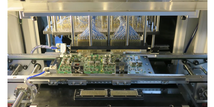
As data centers accelerate into the 800G and even 1.6T era, optical modules—“the heart” of network connectivity—directly determine bandwidth and stability. Behind that, PCB design and manufacturing play a critical role. But designing a PCB that meets electrical specs is not enough. How do you ensure that after complex assembly, it still meets strict electro‑optical performance and thermal-management targets? That’s where Fixture design (ICT/FCT) delivers core value. A great test fixture is not only the quality “gatekeeper” on the production line, it’s also the bridge between simulation and real product performance—ensuring every module that passes SMT assembly can operate stably in real conditions.
From a connector and fiber‑optic engineer’s perspective, this article breaks down Fixture design (ICT/FCT) for data center optical-module PCB testing. We explain how to balance high-speed signal integrity, precision thermal management, materials science, and system-level airflow—and how fixtures work together with First Article Inspection (FAI) and Flying probe test to achieve reliable volume production of high-performance optical modules.
Core challenges of Fixture design (ICT/FCT): the dual battle of high-speed signals and thermal management
For optical modules, fixture design is far more than simple electrical connection. It’s a complex system engineering task that must solve two contradictions simultaneously: preserve 112G PAM4 signal integrity and provide precise thermal management for modules with power above 20 W.
1. High-speed Signal Integrity challenges
In in-circuit test (ICT) and functional test (FCT), the fixture connects to the DUT through pogo pins or dedicated connectors. These physical connections become part of the high-speed channel. Any impedance mismatch, crosstalk, or loss directly affects measurement accuracy—and can even cause false failures.
- Impedance control: from probes and interposer boards to cables, the whole fixture channel must maintain strict 50 Ω single-ended or 100 Ω differential impedance. Fixture design typically uses 3D EM simulation to calculate probe pitch, trace geometry, and ground return paths to minimize reflection (jitter) and insertion loss.
- Low-loss materials: the fixture’s internal PCB and connectors must use ultra-low-loss materials—often better than the product’s own High-Speed PCB materials—so the test system doesn’t become the performance bottleneck.
- Probe selection and layout: high-frequency probes must have low inductance, wide bandwidth, and stable contact resistance. Layout must avoid electromagnetic coupling between probe fields.
2. Thermal Management challenges
Modern optical modules—especially QSFP-DD and OSFP—integrate high-performance DSP, drivers, and lasers, pushing power higher every generation. In FCT, modules often run at full load to validate eye diagrams, BER, and other key metrics. The fixture must therefore simulate (or outperform) the final application’s cooling.
- Emulating real cooling conditions: an ideal FCT fixture mimics the thermal boundary conditions in the final chassis, including contact thermal resistance to the heat spreader and surrounding airflow.
- Integrating active cooling: for high-power modules, fixtures commonly integrate fans, heat pipes, or even miniature liquid cooling to keep the DSP and laser temperature within spec.
- Temperature monitoring: fixtures should integrate thermocouples/sensors to track key locations in real time and feed data back to the test system for correlation and over-temperature protection.
Across the flow, Fixture design (ICT/FCT) is the key step that validates SMT assembly quality. Early Flying probe test can only detect opens/shorts on a bare or lightly assembled board; functional validation depends on a well-designed fixture.
TEC and heat-path coordination: complete thermal-flow management from die to heatsink
Optical-module long-term reliability depends heavily on stable internal temperature—especially for DML/EML lasers that require tight wavelength control. The Thermo-Electric Cooler (TEC) is the core component for active temperature control, but its efficiency depends on a continuous end-to-end “heat path” from chip to the final heatsink. FCT fixture design must deeply participate in validating this full thermal-flow system.
1. Device–PCB–heatsink heat-path analysis
A typical heat path contains multiple segments; each segment’s thermal resistance impacts overall cooling efficiency:
- Die to package: the heat source (DSP/laser) conducts heat through TIM to the lid/substrate.
- Package to PCB: the package transfers heat to surface copper through solder joints or thermal adhesive.
- In-board conduction: heat spreads through large copper planes (heat spreader) and dense thermal-via arrays to conduct efficiently through the Z axis. This is the essence of High-Thermal PCB design.
- PCB to heatsink: the PCB backside contacts an external heatsink (module case or saddle heatsink), and via TIM the heat is ultimately rejected to air.
2. What the FCT fixture validates
An FCT fixture does more than power the DUT—it acts as a “temporary heatsink”. A precisely designed thermal block presses onto the module PCB’s dedicated thermal region to emulate the final heatsink’s heat-sinking behavior.
- TEC control stability testing: the fixture must provide TEC with stable, low-noise power and monitor drive current and ΔT. Running FCT under different ambient temperatures validates control-loop stability and confirms the laser temperature can be locked precisely.
- Thermal-via array validation: combined with FCT, IR thermography can clearly show whether heat is evenly extracted through the thermal-via array. If via design or fabrication deviates and is caught in First Article Inspection (FAI), thermal images will reveal localized hot spots.
Table 1: comparison of thermal-management approaches for optical-module PCB
| Approach | Core principle | Advantages | Challenges & fixture-design notes |
|---|---|---|---|
| Thermal-via array (Thermal Vias) | Uses plated vias to build a low thermal-resistance path in the Z direction. | Low cost and compatible with standard PCB processes. | Efficiency depends on via density/diameter and copper filling. The FCT fixture must align precisely to the heat-spreading region. |
| Embedded copper coin (Embedded Coin) | Embeds a solid copper slug in the PCB stackup under key devices. | Extremely low thermal resistance and very high heat-removal efficiency. | Complex process and higher cost; CTE matching is critical. The fixture must ensure good contact to the copper coin. |
| Thermo-electric cooler (TEC) | Uses the Peltier effect to actively pump heat from one side to the other. | Enables precision temperature control, even below ambient. | Consumes extra power; hot-side cooling is the key. The fixture must provide stable power and cooling for the hot side. |
| Heat pipe / vapor chamber (Heat Pipe/VC) | Uses phase-change heat transfer to move heat quickly over distance. | Very high effective thermal conductivity; rapidly equalizes hot spots. | Requires additional mechanical integration space. The FCT fixture should simulate the final integration method with the PCB. |
CTE matching and low warpage: protecting fiber-coupling efficiency and assembly yield
The core of an optical module is electro‑optical conversion. Performance depends on micron and even sub‑micron alignment—for example, coupling between the laser and the fiber array. PCB thermally induced deformation (warpage) is the “natural enemy” of that precision. CTE mismatch is the primary driver of warpage.
- Root causes of CTE mismatch: optical-module PCB integrate multiple materials—FR-4 or advanced resin systems, copper foil, ceramic packages, metal housings, etc.—with different CTE. During SMT assembly reflow or high-temperature Selective wave soldering, and during operational temperature swings, inconsistent expansion/shrink creates internal stress that bends or twists the PCB.
- Warpage impacts:
- Fiber-coupling loss: warpage shifts the optical engine’s position/angle, sharply reducing coupling efficiency and degrading signal quality.
- Assembly difficulty: warped PCB are hard to install into the module housing and may create poor heatsink contact (air gaps), severely hurting cooling.
- Solder-joint reliability: long-term stress cycles accelerate fatigue failures on critical joints such as BGA.
Design and test strategy
To manage this challenge, you must address it across materials, stackup design, and verification:
- Material selection: choosing low-CTE cores and prepregs is fundamental. Filled high-performance resins can bring X/Y CTE closer to ceramic/semiconductor materials and reduce stress.
- Symmetric stackup design: in HDI PCB stackups, strict symmetry is required—mirror dielectric thickness, copper thickness, and routing density around the center plane to balance internal stress and suppress warpage.
- How FCT fixtures validate warpage control: fixtures matter. With precision locating pins and clamping blocks, the fixture holds the PCB in an ideal plane. By running functional tests at different temperatures, engineers can quantify how warpage affects electro‑optical performance. A module that passes at room temperature but shows BER spikes at high temperature is often suffering optical-path misalignment caused by thermal warpage.
Airflow and pressure-drop (ΔP) optimization for QSFP-DD/OSFP cages
Once the module PCB is assembled and placed into the test fixture, you should consider not only the PCB, but also the final system environment. In a data center rack, dozens of QSFP-DD/OSFP modules are inserted side by side, creating a dense thermal zone. Module cooling depends not only on the heatsink itself, but also on complex airflow and system impedance (pressure drop ΔP).
1. System-level airflow analysis
- Channel effect: dense module arrays form narrow cooling channels. Hot exhaust from upstream modules heats downstream modules, raising inlet air temperature far above rack inlet temperature.
- Pressure drop (ΔP): airflow sees resistance through heatsink fins, PCB components, and cage vents, causing pressure loss. Total fan static pressure must overcome ΔP across the entire path. If a single module heatsink is too dense (to maximize area), its high ΔP can “steal” airflow and worsen cooling of adjacent modules.
2. How an FCT fixture simulates the system
Advanced Fixture design (ICT/FCT) incorporates system-level factors by working with wind tunnels and related equipment to create more realistic validation.
- Integrated wind-tunnel testing: the FCT fixture can be built as a test module that mounts in a small wind tunnel. By controlling air speed and inlet temperature precisely, you can simulate different rack positions and fan-speed conditions.
- ΔP measurement: pressure sensors at inlet/outlet of the fixture measure module ΔP under a given air speed. This data is critical to system thermal designers selecting fans based on total ΔP across all modules.
- CFD correlation: design teams often use CFD to simulate thermal performance. Wind-tunnel FCT data is the most direct way to validate and calibrate CFD models.
System-level validation prevents the trap of “optimized module, failing system” and ensures reliable operation in harsh data center conditions. The rigor of this step is also a key measure of professionalism for a Turnkey Assembly provider.
Design reminders: coordinated thermal + airflow design for optical-module PCB
- Component layout optimization: place primary heat sources (DSP, etc.) on the windward side or in the strongest airflow region. Avoid tall components (e.g., electrolytic capacitors) blocking airflow paths around critical devices.
- Heatsink and cage coordination: align fin orientation with the cage’s main airflow direction to reduce ΔP, and consider bypass airflow between the heatsink and cage.
- Laminate and copper-thickness selection: while meeting signal integrity, increasing copper thickness on ground/power planes can significantly improve in-board conduction and temperature spreading.
- Early validation: don’t wait until prototypes are complete to run thermal testing. Evaluate during design using simulation tools, and use First Article Inspection (FAI) to verify the physical build matches the design.
Thermal-test validation: from IR imaging to full functional environmental testing
Design and simulation are theory—only rigorous physical testing provides final confidence. The ultimate goal of Fixture design (ICT/FCT) is to offer a stable, controllable, and efficient platform for these validation methods. A complete thermal-validation flow typically includes:
1. Infrared imaging
IR cameras capture PCB surface temperature distribution without contact—ideal for spotting hot spots and evaluating heat-path efficiency.
- Fixture design requirements: to enable IR viewing, the fixture structure above the module should minimize blockage, and may include dedicated viewing windows. In some cases, thermal blocks and clamps must be temporarily removed and IR images captured quickly (before thermal saturation).
- Analysis value: IR images show whether heat spreads uniformly from under the DSP through thermal vias, whether the TEC hot/cold sides have a clear ΔT, and whether auxiliary heat sources (e.g., DC/DC) stay within expected temperature. Abnormal local hot spots can indicate design issues or solder defects during SMT assembly.
2. Multi-point thermocouple measurement
IR imaging is intuitive but accuracy depends on emissivity. More accurate temperature data comes from micro thermocouples attached to key devices (DSP surface, laser case, PCB hot spots).
- Fixture integration: the FCT fixture must provide fine routing channels to bring thermocouple leads out to data-acquisition equipment without interfering with module mounting or airflow.
- Correlation analysis: the test system correlates multi-point temperature data with optical-module parameters (optical power, BER, power consumption) in real time, producing performance‑vs‑temperature curves and defining safe operating limits.
3. Full functional environmental testing
This is the most demanding test, simulating environmental temperatures over the module lifecycle.
- Test flow: place the entire FCT fixture (with DUT installed) into a thermal chamber. The program controls chamber temperature; after stabilizing at set points (e.g., -5°C, 25°C, 70°C), it runs the full functional test suite.
- Fixture robustness across temperature: fixture materials, cables, probes, and moving parts must operate stably across wide temperature ranges without contact failures caused by thermal expansion/shrink.
- Purpose: environmental testing exposes issues not visible at room temperature—component parameter drift at low temp, performance degradation due to CTE mismatch at high temp, and long-term reliability of connectors assembled via THT/through-hole soldering under temperature cycling.
From early Flying probe test for basic connectivity, to First Article Inspection (FAI) for physical implementation accuracy, to full electrical/thermal/environment validation via precision Fixture design (ICT/FCT)—this is a tightly coupled quality chain.
Conclusion: the test fixture is the final gate between design and reality
In data center optical modules—where optics, electronics, thermals, and precision mechanics converge—PCB have long gone beyond simple interconnect. They become the foundation of system performance and reliability. Fixture design (ICT/FCT) is the final safeguard that keeps that foundation solid.
A successful fixture design reflects deep understanding of high-speed signals, thermodynamics, materials science, and system environment. It must be electrically “transparent”, thermally “realistic”, and mechanically “stable”—ensuring that every PCB from lab to volume production, whether it went through complex SMT assembly or precision THT/through-hole soldering, performs consistently with design intent.
At HILPCB, we believe advanced test capability is indispensable for high-end PCB manufacturing and assembly. Beyond industry-leading SMT Assembly, we engage early with customers to discuss DFT and co-develop test approaches that reflect real operating conditions. Because we believe excellent Fixture design (ICT/FCT) is not only a production tool—it is the final protection of your product performance and market promise.
Common Questions
Why must optical-module fixtures be electrically transparent and thermally realistic?
Because the module’s measured behavior depends heavily on the surrounding test environment. If the fixture adds loss, noise, unstable contacts, or unrealistic cooling, the results will not represent how the optical module behaves in actual service.
Why should optical, electrical, and thermal measurements be combined in one fixture strategy?
Optical modules are tightly coupled systems where laser output, DSP behavior, power consumption, and temperature all affect each other. A fixture strategy that separates those factors too much can miss the real root cause of margin loss or instability.
Why are environmental testing and contact stability important for these fixtures?
Optical modules often need to perform across a wide temperature range and through many insertion cycles. The fixture therefore has to maintain stable probing, signal paths, and mechanical alignment even when temperature and handling conditions change.
How does early fixture planning reduce risk from prototype to volume production?
It helps teams define DFT access, thermocouple routing, chamber-ready setups, and repeatable functional measurements before validation gets expensive. That reduces redesign work and makes it easier to scale from first samples to production screening.