
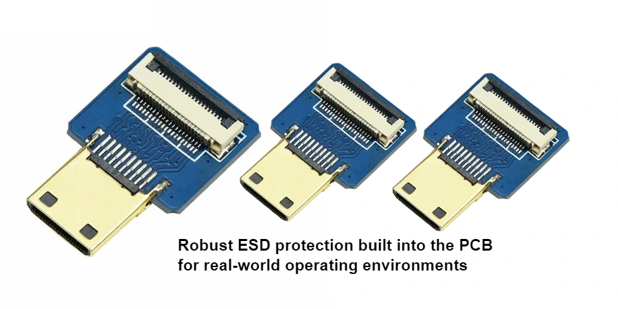
ESD protection is non-negotiable for HDMI ports. Cable hot-plug, human touch near the connector, and charged cables in dry environments can damage an HDMI interface immediately—or cause latent degradation that only appears later as “sparkles”, intermittent black screens, EDID/CEC instability, or increased EMI failures.
This guide explains how to build real-world HDMI ESD protection that does not compromise signal integrity. It covers TVS selection for high-speed lanes, low-inductance layout rules (the part that makes or breaks protection), grounding strategies, cable discharge event (CDE) considerations, EMI/common-mode filtering, and practical validation steps.
If you want the shortest rule of thumb:
Connector → TVS → Ground (very short) → IC (protected).
Most ESD failures happen because the TVS ground return is too inductive or the signal reaches the IC before the TVS can clamp.
Understanding ESD Threats on HDMI Ports (HBM, CDE, System-Level)
HDMI connectors face ESD from several sources, and each stress type behaves differently:
- Human-body contact during insertion (HBM-like / IEC gun events): fast rise time, short duration; commonly tested with IEC 61000-4-2 style methods.
- Cable Discharge Event (CDE): a charged cable dumps higher energy into the connector; often more damaging than “typical” human contact.
- System-level ESD (chassis/metal enclosure events): discharge to the chassis couples into the port through grounding paths.
- Indirect coupling (nearby ESD): common-mode noise can couple into the high-speed pairs and trigger link instability.
ESD protection effectiveness depends on component choice + layout inductance, especially the ground return path and how close the TVS sits to the connector.
Typical failure patterns you’ll see in the field
- Immediate catastrophic failure: TVS short, connector pin short/open, or HDMI IC failure.
- Latent damage: increased leakage, reduced margin, intermittent link failures days/weeks later.
- Pin vulnerability: HPD and DDC lines are frequently hit due to handling and first-contact behavior; +5V can be abused by powered sinks.
TVS Diode Selection for HDMI (High-Speed Lanes vs. Control Pins)
TVS devices for HDMI must balance three competing requirements:
- Fast response and low dynamic resistance (for effective clamping)
- Low capacitance (to avoid loading high-speed lanes)
- Adequate surge/ESD current rating (to survive repeated hits)
Different HDMI pins have different priorities.
1) High-speed lanes (TMDS / FRL)
High-speed lanes are the most sensitive to capacitance and discontinuities.
What to look for
- Ultra-low capacitance (typical target: sub‑pF per line; keep total loading per differential pair low)
- Low clamping voltage compatible with your HDMI IC absolute maximum ratings
- Bidirectional protection (for both polarities) unless the interface requires otherwise
- Low-leakage at normal operating voltage
- Package and pinout that supports short routing right behind the connector
Practical tip:
Capacitance specs can vary with bias voltage and frequency. Always check the datasheet test conditions and derating curves.
2) DDC (SDA/SCL), HPD, CEC
These are low-speed / control lines and tolerate higher capacitance than high-speed lanes.
What to look for
- Standard low-cost TVS parts or multi-channel arrays often work well
- Clamping voltage appropriate for 5V-domain signals
- Bidirectional behavior for SDA/SCL and CEC is commonly preferred (design-dependent)
3) +5V rail protection
The +5V pin often needs both overcurrent and overvoltage protection:
- PPTC resettable fuse for overcurrent
- Unidirectional TVS for overvoltage spikes
- Optional reverse protection if your use case includes “hot-plug abuse”
HDMI ESD Layout: Placement and Grounding Rules That Actually Work
Even the best TVS does little if your layout creates a long, inductive discharge path. The goal is to provide the lowest-inductance path from the connector to the TVS to ground—and to keep the clamped current away from sensitive circuits.
Key layout rules (high impact)
Place TVS as close to the connector as possible.
Put the array directly behind the HDMI connector pins (keep the unprotected trace length minimal).Route topology must be: HDMI Connector → TVS → HDMI IC
Never route to the IC first and “add TVS later.”Use multiple ground vias at the TVS ground pin.
Parallel vias reduce inductance dramatically. Place them right next to the TVS ground pad.Keep the TVS ground connection short and wide.
Avoid narrow “necked” ground traces. Use a wide stub into a via field.Avoid plane splits under the protection area.
A split ground plane can force ESD current to find longer return paths and raise the clamp voltage seen by the IC.
If your HDMI design is high-density, consider structuring the connector breakout using HDI PCB technology to reduce stub length and routing detours around the TVS area.

HDMI Port Protection Architecture: Signal-by-Signal Circuits + Cable Discharge Event (CDE) Hardening
HDMI ESD protection is most reliable when it’s designed as a complete port architecture, not a single TVS “add-on.” Each pin group behaves differently (high-speed lanes vs. control vs. power), and real-world failures are often driven by Cable Discharge Event (CDE)—a higher-energy stress that can overwhelm weak TVS choices or inductive ground returns. Below is a practical, production-proven approach that combines signal-by-signal protection topologies with CDE hardening strategies.
Key Protection Techniques (TMDS/FRL + DDC + HPD + +5V + CDE)
TMDS/FRL Differential Pairs (High-Speed Lanes):
Use ultra-low-capacitance TVS arrays and keep protection fully symmetrical. Protect P and N equally to avoid imbalance, keep pair geometry consistent through the protection region, and avoid asymmetric vias or stubs that can cause mode conversion and reduce margin. Place the TVS as close to the connector as possible, and keep the TVS ground return extremely short with multiple vias.DDC (I²C: SDA/SCL) and CEC (Control Lines):
Protect these lines with TVS/arrays appropriate for the voltage domain, but keep functional behavior stable by placing pull-ups on the protected (IC) side of the TVS. If ringing or overshoot is observed, add small series resistors as needed (value depends on layout and sink behavior). This approach improves robustness without creating false edges or communication instability.HPD (Hot Plug Detect):
HPD is frequently exposed during handling and hot-plug. Add a small series resistor to limit surge current during ESD and reduce stress on the TVS/IC input. Keep HPD protection close to the connector so the transient is clamped before it reaches sensitive circuitry.+5V Pin (Power Rail at the Connector):
A robust sequence is PPTC resettable fuse → TVS → load to handle both overcurrent and overvoltage transients during plug events. If your product has multiple power paths (e.g., USB-C docks, adapters, or shared rails), validate +5V behavior during hot-plug to avoid backfeeding, latch-up, or nuisance resets.CDE Hardening (The “Real-World” Stress Many Designs Miss):
CDE occurs when a cable becomes charged through handling and discharges during insertion, often delivering higher energy and longer ringing than typical contact events. To survive CDE:- Choose TVS parts for survivability, not only lowest capacitance (balance SI and robustness).
- Prioritize an ultra-low-inductance TVS ground return (multiple ground vias right at the TVS pad is often the real fix).
- Implement a chassis/shield discharge strategy so CDE energy prefers the enclosure path instead of the signal ground and IC.
For products with longer internal routing or multiple HDMI ports (switch/matrix/capture devices), stable plane structure and consistent stackups help both SI and robustness; pairing the protection architecture above with multilayer PCB fabrication can improve repeatability across builds.
EMI and Common-Mode Filtering (When to Add a CM Choke)
ESD protection and EMI control often interact. A design that survives ESD may still fail EMC due to common-mode radiation on the high-speed pairs.
When CM chokes help
- Strict EMC targets (consumer Class B, industrial limits)
- Long HDMI cables in noisy environments
- Marginal SI/EMI margin after initial testing
Placement guideline
- Typically between the TVS and the HDMI IC (device-dependent)
- Maintain differential impedance through the choke footprint
- Keep the routing symmetrical across all protected pairs
If your design mixes HDMI with RF/Wi‑Fi/Bluetooth or other high-frequency modules, consider consulting high-frequency PCB options for noise control strategies and stackup planning.

HDMI Shield Grounding: Simple Options and When to Use Them
HDMI shell grounding is often the difference between “passes ESD” and “fails intermittently”.
Common approaches
- Shell tied to signal ground (direct): simplest, often acceptable
- Shell to chassis ground (preferred when enclosure available): best for dumping ESD to the enclosure path
- AC-coupled shell to signal ground: used to reduce low-frequency ground loops while maintaining high-frequency discharge path (must be designed carefully)
Practical rule:
If your product has a metal enclosure or a defined chassis ground, giving ESD a low-impedance chassis path is often beneficial.
Validation and Debug: How to Know Your HDMI ESD Protection Works
Protection without testing is guessing. Validate early—especially if you use different cable types or your product is installed in harsh environments.
Test methods (typical)
- IEC 61000-4-2 contact and air discharge as required by your product spec
- CDE-style test (charged cable plug-in), if your field environment suggests it
- Monitor link behavior during and after strikes (not just “does it still power on”)
Quick debugging map
- IC damage despite TVS present: ground return inductance too high → add vias, shorten/straighten ground path
- TVS fails short: TVS energy rating too low or CDE too severe → choose a stronger part and improve discharge path
- Signal integrity worsens: TVS capacitance too high → lower-capacitance array and improve layout symmetry
- ESD passes but EMI fails: add CM choke or improve shield/chassis grounding
HDMI ESD Design Checklist (Release-Ready)
Component selection
- Ultra-low capacitance TVS for high-speed lanes (TMDS/FRL)
- TVS or arrays for DDC/HPD/CEC appropriate to voltage domain
- +5V rail protected with PPTC + unidirectional TVS (as needed)
- Second-source options identified for key protection arrays
Layout
- TVS placed right behind connector pins
- Topology: Connector → TVS → IC (no bypass)
- Multiple ground vias at TVS ground pad, very short/wide ground stub
- No plane splits under TVS/connector region
- Symmetric routing through protection region for differential pairs
Manufacturing / assembly readiness
- Footprints verified for assembly (fine pitch arrays, tiny packages)
- DFM review done for the connector + protection region
- Protection parts available for your build schedule
HILPCB supports precise placement of TVS arrays and small protection components with SMT assembly services, and can scale builds from early validation to production using small-batch assembly.
Conclusion
HDMI ESD robustness is won or lost at the connector: the right TVS, placed correctly, with a truly low-inductance discharge path. If you combine (1) correct device selection for high-speed vs. control signals, (2) strict placement/grounding rules, (3) sensible shield/chassis grounding, and (4) validation that reflects your real environment (including CDE risk), you can significantly reduce HDMI field failures without sacrificing signal integrity.
If you need support building HDMI boards end-to-end—from controlled stackups to protection assembly—HILPCB can help with standard material builds like FR‑4 PCB fabrication and full turnkey assembly when you want one supplier responsible for PCB + parts + PCBA.