
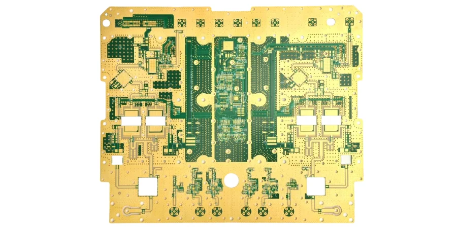
Electroless nickel/immersion gold (ENIG) is a comparatively planar solderable finish: nickel covers the exposed copper pads, and a thin immersion-gold layer protects the nickel before assembly. It is useful when fine-pitch pad flatness, handling and the planned assembly sequence justify its cost. HILPCB offers ENIG alongside OSP and immersion silver on its multilayer PCB route, with other finishes reviewed for the application.
The choice depends on what the finished surface must do. A solder pad, an exposed RF conductor, a wire-bond pad and a repeatedly mated contact have different requirements. Select the finish with the stackup and assembly plan rather than treating a gold appearance as a reliability rating.
What is Immersion Gold PCB?
ENIG uses electroless nickel followed by immersion gold over the exposed copper. The nickel acts as a barrier and provides the surface to which the solder joint forms; the thin gold generally dissolves into the solder during assembly. Its purpose is to preserve a suitable surface before soldering, not to remain as a durable gold coating over the completed joint.
The IPC-4552B public scope identifies soldering, specific wedge-wire bonding and contact applications. It also makes process control, reproducible thickness measurement and uniform deposits central to performance. Specify the applicable IPC-4552 revision and acceptance requirements on the drawing or purchase specification; a visual gold-color check cannot establish those properties.
Benefits of Immersion Gold PCB
1. Flat Pads for Fine-Pitch Soldering
ENIG avoids the solder-coating height variation associated with HASL and provides a useful surface for BGA, QFN and other fine-pitch assembly. Pad design, paste, stencil, placement, profile and nickel-deposit quality still need to work together. Select ENIG for the assembly problem it solves rather than expecting it to correct a poor land pattern or profile.
2. Oxidation Protection Before Assembly
The gold cap protects the underlying nickel against oxidation/passivation during its intended handling and storage life. It is thin and not an impervious environmental seal. Keep packaging, humidity, handling and the permitted time to assembly in the build plan; an exposed ENIG board may still need an enclosure, coating or other protection in service.
3. A Finish That Can Support the Planned Assembly Sequence
ENIG can be a candidate for double-sided assembly or other staged soldering operations when the process is qualified. Count the actual thermal exposures, including rework, and confirm solderability after the required sequence. It is not a wear-resistant hard-gold finish for unlimited mating cycles or a guarantee that solderability remains unchanged throughout the product lifetime.
4. Compatibility with Dense Designs, with RF Review Where Needed
A flat finish is useful on dense communication and digital boards, but ENIG is not automatically the lowest-loss RF finish. The nickel layer and the length of exposed finished conductors can affect loss. Compare the actual finish stack in the channel or RF layout, particularly on exposed transmission lines, launches and antennas. HILPCB’s high-frequency route evaluates finish against the application; a masked digital trace and a long exposed RF trace need different analysis.
5. Compatibility with Automated Assembly
Consistent pad geometry and a controlled finish support repeatable paste printing and placement. Connect finish inspection with assembly inspection and the approved profile. This gives production a usable acceptance basis without attributing the entire first-pass yield to one plating choice.
Applications of Immersion Gold PCBs
- Telecommunications: Fine-pitch processors, transceivers and connectors may benefit from planar solder pads. For satellite or terrestrial RF circuits, review exposed-conductor loss and the environmental plan separately.
- Medical devices: Diagnostic, patient-monitoring and surgical-equipment electronics can use ENIG where their assembly and cleaning requirements support it. The finish is one part of the device’s manufacturing and validation plan.
- Consumer electronics: Smartphones, laptops and wearables often have dense assembly where pad flatness matters. Compare ENIG with the available OSP or other route against the actual package mix, handling and cost.
- Automotive electronics: Control, sensor and power boards need finish compatibility with their soldering, thermal cycling and environment. Automotive use alone does not select a finish or demonstrate its qualification.
- Industrial electronics: Controllers and instrumentation may require planned storage, repair or connector exposure. Distinguish solderable pads from wear contacts and define the evidence needed for each.
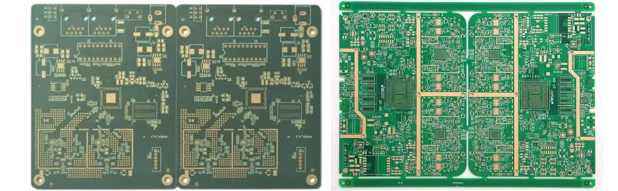
Comparing Immersion Gold to Other Surface Finishes
Immersion Gold vs HASL
HASL can be economical where component pitch and pad geometry tolerate its solder-coating topography. ENIG is a stronger candidate when that height variation creates a printing or fine-pitch placement problem. Compare the specified lead-free or tin-lead HASL alloy, allowed thermal exposure, component mix and accepted assembly cost. A higher finish price can be justified by a specific process benefit; it does not prove longer field life.
Immersion Gold vs OSP
OSP preserves the copper surface for soldering and can also be planar and suitable for demanding assemblies. Compare the selected OSP process with ENIG for handling, storage, the number and order of thermal exposures, probing and rework. Neither automotive nor telecommunications use makes OSP inherently unsuitable. For sensitive exposed RF conductors, include the effect of ENIG’s nickel in the comparison rather than assuming gold must give lower loss.
Contacts and Wire Bonding Need Their Own Specification
For repeated insertion or sliding wear, evaluate a specified hard-gold/contact construction rather than using ordinary thin ENIG by default. For wire bonding, state the wire material, diameter, wedge or ball process and acceptance method. ENIG’s supported wedge-bond applications do not establish compatibility with every gold-wire ball-bond process; an ENEPIG or other qualified finish may be appropriate. HILPCB lists ENEPIG and hard/soft gold as reviewed options on the multilayer route, not as interchangeable substitutes.
Build an ENIG PCB with HILPCB
HILPCB can combine finish selection with multilayer fabrication and turnkey assembly, including approved sourcing, SMT/THT, programming and defined inspection/test records. The manufacturing routes also include heavy-copper, flex and rigid-flex constructions. For ceramic or IC-substrate work, identify the metallization and bonding process so the finish can be reviewed for that construction. HILPCB's experienced engineers can work with customers on ENIG finish selection and design optimization for eligible complex builds, including the heavy-copper, flex and rigid-flex routes described above; the stackup, metallization and assembly sequence determine feasibility.
Send the fabrication files, stackup, pad/package details, quantity and assembly stage with the finish specification. Include the applicable standard revision, nickel/gold deposit requirements and units, locations to be measured, storage/packaging needs and planned reflows/rework. Add any exposed RF conductors, wire-bond pads or mating contacts so those surfaces receive the right review.
Agree the finish-thickness, solderability and nickel-corrosion acceptance evidence and the associated lot records at quotation. Uyemura’s corrosion-control discussion explains why excessive nickel corrosion needs process control and disposition; more gold is not a universal cure for black-pad risk. For repeat orders, retain the approved finish and assembly baseline and review any proposed change before release. This lets purchasing compare the same build scope across quotes and production lots.
Common Questions
What are the main advantages of immersion gold PCB finish?
ENIG offers comparatively flat solder pads and protects the underlying nickel before assembly. It is useful for fine-pitch assembly when the deposit, handling and soldering process meet the agreed requirements.
When is immersion gold a better choice than HASL or OSP?
Choose it when a specific requirement—such as HASL topography, planned handling or a qualified assembly sequence—justifies it. OSP is also planar; compare the actual processes, package mix, storage and total accepted assembly cost rather than ranking every application by finish name.
Is immersion gold suitable for dense and high-frequency designs?
It can support dense solder-pad layouts. High-frequency suitability is a separate question: assess the nickel-containing finish where it lies in the RF current path, along with geometry, copper and dielectric losses.
Can immersion gold handle multiple reflow cycles and storage?
Define the required number of reflows, rework allowance and storage/packaging conditions, then confirm solderability against that plan. There is no universal number of cycles or shelf life for every ENIG board and assembly process.
What is immersion gold plating, and is it the same as hard gold?
In PCB quotations, confirm whether “immersion gold” means the complete ENIG nickel/gold stack and specify both deposits. Thin immersion gold, electrolytic hard gold and ENEPIG are different finishes with different soldering, bonding and contact-use requirements.