
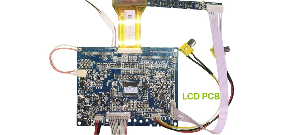
- An LCD controller PCB should be reviewed as an interface and power-delivery board first, not just as a generic display accessory.
- The earliest checks are panel interface type, lane routing strategy, rail sequencing, connector placement, backlight noise isolation, and test access.
- Signal-integrity problems on LCD controller boards usually start with stackup, reference continuity, skew, and connector transitions rather than with the controller IC itself.
- Display quality issues often come from power noise, timing instability, EMI coupling, or poor grounding between the panel, controller, and backlight sections.
- Prototype success depends on aligning fabrication, assembly, and bring-up planning before the first board spin, especially when the design combines fine-pitch packages and high-speed differential pairs.
An LCD controller PCB is the board that receives image data, manages timing and panel interface signaling, generates or distributes the required power rails, and coordinates backlight and control functions for an LCD module. It needs careful review of interface compatibility, routing quality, power behavior, EMI control, and manufacturability because small design mistakes can show up immediately as flicker, instability, or no-display faults.
Contents
- What to review first on an LCD controller PCB
- Key design and manufacturing rule table
- Early engineering trade-off table
- How interface choice affects stackup and routing
- How power rails, backlight control, and EMI interact
- What assembly and prototype teams should verify before release
- FAQ
- Next steps
- References
- Author and review
What to review first on an LCD controller PCB
An LCD controller PCB sits between the image source and the display panel, but it is not just a passive adapter. It usually has to translate interface assumptions into a real physical channel, keep the panel rails stable, manage backlight behavior, and survive dense connector and fine-pitch assembly constraints. It also does not solve every display issue by firmware. If routing, reference planes, sequencing, or grounding are weak, the board can fail before software tuning even begins.The first review points are usually:
- which panel interface the target module actually requires and whether the controller can support it without awkward bridging
- how differential or high-speed lanes will be routed across layers, connectors, and reference-plane changes
- whether the panel power rails, logic rails, and backlight rails need controlled sequencing or isolation
- whether the board outline, connector location, and cable path create EMI or assembly risk
- how the prototype will be inspected, powered up, and debugged if the first article does not display correctly
For dense display control layouts, it is often worth reviewing the stackup against HDI PCB and high-speed PCB capability before layout freeze.
Key design and manufacturing rule table
| Rule / parameter | What to check first | Why it matters | How to verify | If ignored | | --- | --- | --- | --- | --- | | Interface fit | Confirm whether the panel expects LVDS, eDP, MIPI DSI, RGB, or another interface | Wrong interface assumptions force late rework, bridge boards, or unstable timing | Compare panel documentation, controller datasheet, and connector map | No image, unstable link, or heavy redesign | | Stackup and reference continuity | Give high-speed lanes clear return paths and avoid unnecessary plane splits | Signal quality depends on controlled routing and predictable impedance | Stackup review, routing review, [impedance calculator](/tools/impedance-calculator/) check | Reflection, skew, EMI, intermittent display faults | | Power sequencing | Review the order and stability of panel, logic, and backlight rails | Some panels are sensitive to power-up and power-down behavior | Schematic review, oscilloscope bring-up plan, prototype validation | Flicker, latch-up risk, panel stress, startup failure | | Connector and cable transitions | Treat the connector as part of the signal channel, not as a neutral mechanical part | Fine-pitch connectors and flex links can become the weakest SI and reliability point | Footprint review, mechanical fit review, first-article inspection | Signal loss, intermittent contact, assembly yield issues | | Backlight noise isolation | Separate LED drive noise from sensitive logic and video paths | Backlight PWM and power switching can inject noise into the image path | Layout zoning, grounding review, powered prototype test | Brightness instability, visible noise, EMI problems | | Test access | Decide how rails, reset lines, control buses, and display links will be measured | Bring-up becomes slow and error-prone without a debug path | DFT review, test-point planning, prototype checklist | Long debug cycles and avoidable board respins |Early engineering trade-off table
| Design choice | Usually stronger for | Main trade-off | What to confirm early | | --- | --- | --- | --- | | LVDS | Mature industrial and embedded display links | More pins and interface overhead than newer serial links in some cases | Connector count, lane routing space, EMI margin | | eDP | Higher integration and modern panel ecosystems | Depends heavily on channel quality and controller-panel compatibility | Lane budget, AUX handling, connector path | | MIPI DSI | Compact mobile or highly integrated display modules | Can tighten routing, flex, and controller compatibility constraints | FPC path, stackup, lane escape strategy | | Separate backlight board | Cleaner partitioning of noisy power stage in some products | More interconnects and mechanical complexity | Cable path, harness cost, enclosure space | | Integrated backlight drive | Fewer boards and simpler module packaging | More local heat and noise coupling on the controller PCB | Thermal plan, grounding, EMI containment |How interface choice affects stackup and routing
The board architecture should start from the real display interface, not from whatever controller chip is easiest to source. LVDS, eDP, and MIPI DSI each create different routing density, connector, and debug constraints. The question is not which interface is "best" in general. It is which one matches the target panel, cable path, enclosure, and production risk of the product.Three layout decisions usually dominate the outcome.
1. Lane escape and reference quality
If high-speed lanes leave a fine-pitch controller package and immediately cross splits, neck down too aggressively, or change layers without a return-path plan, the design starts with avoidable signal loss and skew. For denser escape regions, HDI PCB routing can reduce compromises, but only if the stackup and via strategy are decided early.
2. Connector and flex transition behavior
The connector to the panel or flex cable is part of the channel. Misaligned pin mapping, poor grounding around the connector, or mechanically weak support can cause intermittent display faults that look like firmware or panel defects. Before release, teams should inspect the physical path in a Gerber viewer rather than reviewing only schematic connectivity.
3. Board outline and mechanical coupling
Display-control boards are often constrained by bezels, housing depth, button placement, or fold geometry. That means routing, connector orientation, and keep-outs should be reviewed together with the mechanical team. If the design uses folded interconnects or compact module packaging, rigid-flex PCB may be the better structural option, but only when the bend region and assembly flow are planned as part of the same system.
How power rails, backlight control, and EMI interact
Many LCD controller boards fail because the signal team and power team treat their work as separate topics. In practice, panel timing, logic stability, and image quality all depend on rail behavior, ground quality, and switching noise containment.The most common problem areas are:
- panel and logic rails that come up in the wrong order or droop during image transitions
- LED backlight drive noise coupling into controller, touch, or video sections
- ground returns shared too freely between noisy and sensitive zones
- thermal buildup around PMICs, boost stages, or backlight drivers in compact housings
If the board includes dense control, power conversion, and fine-pitch assembly on one compact outline, the design should be reviewed as one manufacturable system rather than as isolated blocks. That usually means aligning high-speed PCB, SMT assembly, and PCB prototype planning before the first prototype order is sent.
What assembly and prototype teams should verify before release
An LCD controller PCB can look correct in CAD and still create unnecessary pilot risk if the bring-up and manufacturing plan is weak. Before release, teams should confirm both assembly feasibility and a realistic debug path.A practical release checklist usually includes:
- Footprint and connector audit
Confirm orientation, mating assumptions, mechanical support, and assembly access for fine-pitch connectors and display-related parts. - Bring-up measurement plan
Define where rails, reset lines, enable signals, and communication buses will be measured on first power-up. - Prototype inspection route
Decide whether AOI, X-ray, or manual microscope inspection is required for the package mix and connector density. - BOM and substitution control
Check whether oscillators, regulators, connectors, and controller-adjacent passives have approved alternates and stable sourcing. A BOM viewer review can help catch mismatches before purchasing. - Pilot build objective
Separate "display bring-up" prototypes from "production-like" pilot builds so the test depth, documentation, and rework boundaries match the actual goal.
If the board will move quickly from prototype into coordinated sourcing and assembly, turnkey assembly and quick-turn PCB support usually reduce handoff errors compared with splitting fabrication and assembly across disconnected workflows.
FAQ
What is the first thing to check when an LCD controller PCB shows no image?
Start with interface compatibility, rail sequencing, reset state, and connector orientation. Many no-display faults come from basic bring-up conditions rather than from the display controller IC itself.
Is LCD controller PCB design mainly a firmware problem?
No. Firmware matters, but stackup, return paths, skew control, connector transitions, power behavior, and assembly quality often decide whether the hardware can work consistently in the first place.
When is HDI useful for an LCD controller board?
HDI is usually helpful when the controller package is fine-pitch, routing escape is dense, and the design needs to preserve cleaner channel geometry than a conventional breakout can provide.
Should the backlight driver always stay on the same board as the LCD controller?
Not always. Integration can simplify packaging, but it can also increase heat and noise coupling. The better choice depends on enclosure space, EMI margin, thermal path, and serviceability.
What should be frozen before the first prototype release?
Freeze the panel interface choice, stackup assumptions, connector map, power-rail strategy, bring-up test points, and the prototype inspection path.
Next steps
If you are developing an LCD controller PCB, the most useful next step is usually to review the interface channel, power behavior, and assembly path together instead of optimizing each one in isolation.HILPCB can support that process through:
- HDI PCB review when escape routing and fine-pitch density are the main bottlenecks
- High-speed PCB planning when the display channel needs tighter control over routing and reference continuity
- Rigid-flex PCB evaluation for compact or folded display-module architectures
- SMT assembly and turnkey assembly alignment when fabrication, assembly, and first bring-up need to stay coordinated
- PCB prototype and quick-turn PCB support for early validation builds
- Request a quote when your layout package, BOM, and assembly notes are ready for review