
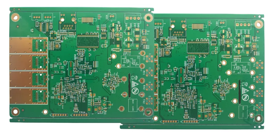
Modern electronics demand circuit boards that deliver higher routing density, cleaner power delivery, and stable high-speed performance in increasingly compact products. From telecom infrastructure and industrial automation to medical imaging and automotive electronics, Multilayer PCB technology is the foundation that enables functions a single- or double-layer board cannot reliably support.
What separates professional Multilayer PCB manufacturing from basic fabrication is repeatability: stable stackups across high layer counts, controlled impedance execution for high-speed interfaces, thermal-aware copper planning, and quality systems that scale from quick-turn prototypes to volume production. At HILPCB, we provide 4–64 layer Multilayer PCB fabrication, optional HDI PCB capability, verification deliverables (such as impedance coupons when required), and integrated PCB assembly services to help teams validate faster and scale with confidence.
Managing Signal Integrity in High-Speed Multilayer PCB Designs
As data rates move into 10Gbps+ territory (PCIe, USB, 100G Ethernet and beyond), Multilayer PCB design and manufacturing must support predictable impedance, controlled crosstalk, and stable return paths. Small deviations in dielectric thickness, copper thickness, or via structures can create link margin issues and slow down product validation.
HILPCB supports high-speed Multilayer PCB builds with stackup planning, process control, and verification options that help engineering teams achieve stable results from prototype to production.
Key Signal Integrity Techniques
- Controlled Impedance Builds: Stackup-driven trace geometry targets for 50Ω single-ended and 100Ω differential routing, with impedance coupon testing available when specified.
- Stackup Architecture for Noise Control: Signal layers placed adjacent to solid reference planes to reduce EMI and improve impedance predictability (stripline/microstrip choices by application).
- Via Strategy and Stub Control: Via design choices that reduce discontinuities; backdrill can be applied when the channel budget requires it.
- Return Path Continuity: Plane planning and stitching strategies that maintain low-inductance return paths through layer transitions.
- Material Strategy for Loss Control: Hybrid stackups and low-loss materials can be applied to critical channels while keeping total cost practical.
- Differential Pair Discipline: Coupling, symmetry, and matching rules implemented in a way that remains manufacturable at scale.
Performance Validation and Compliance
For high-speed projects, the goal is not only “meeting a target on paper,” but achieving repeatable electrical behavior across lots. With the right stackup execution, via control, and verification deliverables, teams can reduce SI-related respins, shorten debug cycles, and improve first-pass compliance readiness.
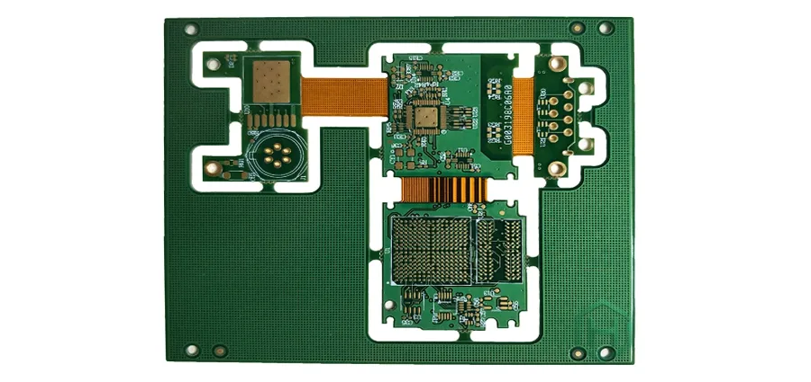
Optimizing Power Distribution Networks in Complex Multilayer Stackups
A reliable Power Distribution Network (PDN) is a core advantage of Multilayer PCBs. Modern boards must deliver low-noise power to processors, FPGAs, radios, and mixed-signal blocks while handling fast transient current demands. Poor PDN implementation increases voltage droop, ground bounce, and EMI risk.
HILPCB supports PDN-friendly Multilayer PCB constructions that prioritize stable planes, practical decoupling implementation, and manufacturing-friendly execution.
Key Power Distribution Techniques
- Dedicated Power/Ground Planes: Low-impedance planes for critical rails with controlled segmentation when isolation is needed.
- Decoupling-Friendly Layout Support: Plane structures that support multi-tier decoupling without forcing fragile routing.
- Plane Stitching and Via Planning: Power/ground via arrays that reduce impedance and improve high-frequency return behavior.
- Current Capacity Planning: Copper weight selection based on current density and thermal constraints, including heavy copper PCB options when required.
- Assembly-Ready Plane Connections: Thermal relief tuning that balances solderability and electrical performance for consistent assembly yield.
Power Integrity You Can Scale
A PDN that is designed and manufactured for repeatability reduces system instability during bring-up and lowers the risk of EMI surprises later in validation. For OEM programs, stable PDN execution is one of the fastest ways to improve yield, reduce rework, and keep production output consistent.
Achieving Thermal Management in High-Power Multilayer PCB Applications
As power density rises, Multilayer PCBs must help manage heat—especially in industrial controllers, telecom modules, LED drivers, and computing platforms. Thermal performance depends on copper distribution, via-based heat paths, and materials that remain stable during continuous operation and rework cycles.
HILPCB supports thermal-aware Multilayer PCB builds that improve heat spreading without sacrificing manufacturability.
Key Thermal Management Techniques
- Copper Plane Heat Spreading: Internal plane coverage and copper weight choices that reduce hotspot intensity.
- Thermal Via Arrays: Via patterns beneath power components to connect heat into internal planes or opposite-side copper.
- Material Stability for Long Duty Cycles: Options such as high-Tg PCB materials for better stability in elevated-temperature operation.
- Placement and Heat Path Planning: Practical design feedback that supports real cooling interfaces (heatsinks, chassis contact, airflow).
- Manufacturing-Consistent Execution: Process control that helps thermal behavior remain stable across builds.
Thermal Reliability Outcomes
A predictable thermal design reduces long-term drift, improves component lifetime, and lowers field failure risk. For products shipping into harsh environments, stable thermal execution also helps keep electrical performance within spec under load and across temperature ranges.

Accelerating Development with Quick-Turn Multilayer PCB Prototyping
Prototype speed matters—especially for telecom, industrial, and computing products where timelines are aggressive and iteration is unavoidable. Quick-turn Multilayer PCB capability is most valuable when the prototype process remains faithful to production methods.
HILPCB supports quick-turn Multilayer PCB prototyping (typical 5 working days for common stackups) with DFM review and optional verification deliverables.
Key Rapid Prototyping Capabilities
- Fast DFM Review: Manufacturability checks within 24 hours to reduce fabrication surprises.
- Pre-Qualified Stackups: Standard 4/6/8-layer stackups to start fabrication faster.
- Prototype Impedance Support: Impedance coupons and reporting available when required for high-speed channels.
- Low MOQ Options: Practical quantities for R&D and early validation builds.
- Assembly Coordination: When assembly is required, sourcing and scheduling can be aligned to shorten total cycle time via turnkey assembly.
Faster Iteration Without Compromising Scalability
The best prototypes are not only fast—they are representative. When prototypes follow production-relevant processes, teams can validate decisions earlier and scale with fewer last-minute changes, reducing total development cost and schedule risk.
Ensuring Manufacturing Quality in Multilayer PCB Production
Quality consistency across layer counts and build lots determines product reliability and cost of ownership. Multilayer PCB quality relies on material control, inner-layer inspection, lamination registration, and electrical testing that is applied consistently.
HILPCB operates quality controls designed to support both prototype validation and volume manufacturing stability.
Key Quality Control Measures
- Incoming Material Verification: Laminate/prepreg checks aligned to specifications.
- Inner-Layer AOI: Defect detection before lamination to prevent high-cost scrap later.
- Registration Verification: Controls that support tight alignment on higher layer counts.
- Electrical Testing: Flying probe for prototypes or fixture testing for production, as applicable.
- Impedance Documentation: Coupon-based measurement and reporting when specified.
Quality That Supports OEM Scale
Consistent quality systems reduce escape defects and stabilize yields as volumes grow. For OEMs, predictable build quality also improves cross-team efficiency: fewer line holds, fewer incoming inspection issues, and faster resolution when changes are required.
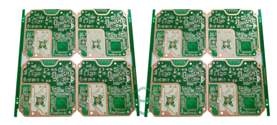
Cost-Effective Multilayer PCB Solutions for OEM Manufacturing
Cost optimization in Multilayer PCB programs is about total value—not just unit price. The most common drivers of cost are layer count, materials, special processes, yield, and test/inspection scope. Strategic choices can reduce cost without sacrificing reliability.
HILPCB supports cost-effective Multilayer PCB manufacturing through collaborative DFM and scalable production planning.
Key Cost Optimization Strategies
- Layer Count Optimization: Reduce layers where possible through stackup and routing planning.
- Standardization Where It Makes Sense: Use standard cores/prepregs and proven build recipes to improve availability and yield.
- Panel Utilization Planning: Better panel yield reduces per-unit cost, especially in mid-volume runs.
- Material Guidance: Use standard FR-4 where sufficient; apply specialty materials only where needed.
- Supply Chain Consolidation: Turnkey delivery via turnkey assembly can reduce coordination cost and shorten schedules.
Total Cost of Ownership Benefits
A stable manufacturing partner reduces hidden costs such as respins, rework, and delivery variability. When DFM, quality, and supply planning are aligned, OEM teams gain predictable outcomes that protect margin across the product lifecycle.
Multilayer PCB Assembly Service and Turnkey Manufacturing
Many programs benefit from a single supplier managing PCB fabrication plus assembly, reducing handoffs and improving accountability. Multilayer PCBs often include mixed technologies: fine-pitch SMT, large connectors, and through-hole power parts.
HILPCB provides integrated assembly workflows combining precision placement and mixed-technology support.
Assembly Capabilities
- Precision SMT Placement: Fine-pitch and small passive support via SMT assembly.
- Mixed Technology Builds: Connectors and power devices supported through through-hole assembly.
- Component Sourcing Options: Procurement aligned to your alternates policy and schedule.
- Inspection and Testing: AOI and test coordination based on your acceptance requirements.
- Documentation Support: Records aligned to QA needs for prototypes and production.
Why Turnkey Improves Delivery
Turnkey manufacturing reduces scheduling friction and keeps revisions aligned across PCB + BOM + assembly documentation. It also speeds issue resolution because fabrication and assembly are managed under one plan, improving time-to-market and production ramp stability.
Conclusion
Multilayer PCB technology enables the high-performance electronics behind telecom infrastructure, industrial automation, medical systems, automotive electronics, and computing platforms. HILPCB delivers scalable Multilayer PCB fabrication (4–64 layers), quick-turn prototyping, optional HDI capability, controlled impedance support, and integrated assembly services to help teams validate faster and manufacture reliably.
Contact HILPCB for Multilayer PCB prototypes, custom fabrication, or turnkey PCB assembly—built for repeatable quality, predictable delivery, and smooth scaling from prototype to volume.