
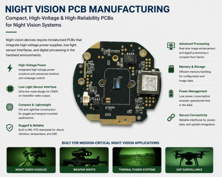
The global night vision device market reached $8.9 billion in 2023 and is projected to exceed $13 billion by 2030, driven by military modernization programs across NATO nations. Night vision devices transform invisible scenes into visible images—either by amplifying ambient starlight through image intensifier tubes (Gen II/III analog technology) or by capturing photons with ultra-sensitive digital CMOS sensors and processing the result electronically. Both approaches place demanding and fundamentally different requirements on the PCB.
Night vision devices are fielded by every NATO infantry force—from the United States Army and Marine Corps to the British Army, German Bundeswehr, French Army, and Canadian Armed Forces. The PCBs must meet manufacturing standards demanded by defense procurement agencies across North America and Western Europe while achieving the miniaturization that soldier-worn equipment requires.
An analog night vision device requires a high-voltage power supply generating 600–900 VDC for the microchannel plate and up to 18,000 V for the phosphor screen—from a 3V battery, within a PCB footprint smaller than a postage stamp, drawing less than 100 mW for 40+ hours of operation. A digital device replaces the tube with a low-light CMOS sensor and processing electronics for real-time enhancement and sensor fusion—requiring high-speed digital processing within the same power-constrained, miniaturized form factor.
HILPCB Manufacturing Capability: We fabricate night vision PCBs with high-voltage insulation rated to 20 kV, ultra-miniaturized HDI construction for goggle-mounted electronics, and flex/rigid-flex configurations for helmet-mounted displays—supporting programs across NATO defense forces.
In This Guide
- Night Vision Technologies: Analog, Digital, and Fused
- Image Intensifier High-Voltage Power Supply PCB
- Digital Night Vision Sensor Interface and Processing
- Miniaturization, Weight, and Power Management
- Environmental Qualification and Production Testing
- HILPCB Night Vision PCB Manufacturing
Night Vision Technologies: Analog, Digital, and Fused
The night vision market is transitioning from pure analog image intensifiers to hybrid digital-analog architectures fusing multiple sensor modalities. Understanding each technology's PCB implications—and their combination in the latest systems—is essential for designing boards meeting current production and future upgrade requirements.Analog Gen II/III systems use vacuum image intensifier tubes. The PCB provides high-voltage power to the photocathode (-600 to -900 V), MCP (800–1000 V), and phosphor screen (5,000–18,000 V), plus automatic brightness control regulating MCP voltage and bright source protection gating the tube against sudden illumination. Gen III devices include auto-gating circuits switching 600–900 V at up to 10 kHz with rise/fall times below 100 ns—requiring low-inductance paths and fast recovery diodes.
Digital night vision uses back-side illuminated CMOS sensors (6–10 μm pitch, >90% QE in near-IR) with real-time processing and micro-OLED display. The latest ENVG-B systems fuse image intensifier and uncooled thermal imagery, performing pixel-level registration of two simultaneous streams—doubling video processing bandwidth and requiring 8–10 layer boards with high-speed interfaces and more powerful FPGA processing.
Image Intensifier High-Voltage Power Supply PCB
The HVPS is among the most space-constrained high-voltage designs in electronics—converting 3V to 18,000 VDC within 20×15 mm. The design must simultaneously achieve voltage ratings normally demanding centimeters of clearance, >90% switching efficiency for battery life, and EMI suppression preventing visible image artifacts.The multi-stage topology includes a boost converter (3V to 12–24V), flyback or resonant converter (1,000–5,000V), and Cockcroft-Walton multiplier ladder to 18,000V. At 18 kV, IPC-2221 requires 25+ mm air clearance—impossible in 20 mm.
At HILPCB, our HVPS fabrication overcomes this through coordinated material and design strategies:
- Conformal Coating/Potting: Increases surface dielectric strength, reducing clearance to 3–5 mm/kV. Board material with CTI ≥600V.
- Inner-Layer HV Routing: High-voltage traces embedded between dielectric on 4–6 layer high-Tg FR-4 with ≥40 kV/mm dielectric strength, low-voltage control on outer layers.
- EMI Containment: Spread-spectrum frequency modulation, multi-stage LC output filtering, and shielded ground planes suppress the 100–500 kHz switching noise that causes visible horizontal bars in the intensifier output.
- Production Validation: Hipot testing at 27 kV (1.5× rated) for 60 seconds, plus partial discharge testing detecting micro-voids that could cause arcing under thermal cycling.
Digital Night Vision Sensor Interface and Processing
Digital night vision requires ultra-clean analog interfaces for the low-light CMOS sensor alongside high-speed digital processing—two domains coexisting on boards small enough for goggle housings without compromising sensitivity or processing capability.Ultra-sensitive CMOS sensors (Teledyne FLIR, Sony Starvis) provide usable imagery below 1 millilux. The interface requires <200 μV power supply noise (multi-stage LDO regulation), LVDS or MIPI CSI-2 output (2–8 lanes at 1–2.5 Gbps), pixel clock jitter <50 ps, and real-time dark current compensation (doubles every 7°C).
The processing FPGA or ISP performs temporal noise reduction (multi-frame averaging for 3–6 dB SNR improvement), bilateral spatial filtering, automatic gain/histogram equalization, and electronic zoom with stabilization. The processing board uses 6–10 layers with HDI for the FPGA package and controlled impedance for high-speed interfaces.
The display driver PCB handles micro-OLED format conversion, brightness control, and ambient-light auto-adjustment, connected to the processor through a flex ribbon. EMI containment is critical—display switching signals must not couple into the sensor or HVPS.
Miniaturization, Weight, and Power Management
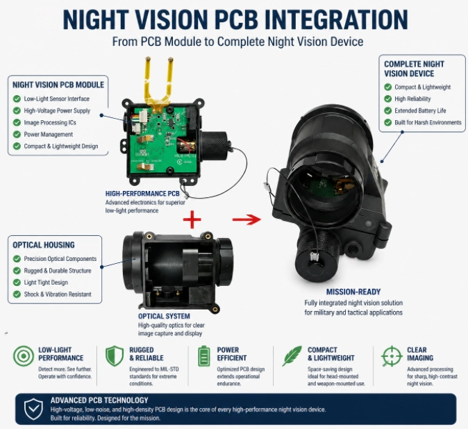
Night vision goggles weigh 450–700 g; NATO STANAG 4695 limits head-borne weight to 680 g including mount and battery. Every gram of PCB weight affects soldier comfort and operational endurance. The design must simultaneously minimize weight, maximize battery life, and maintain optical alignment precision.HDI with laser-drilled microvias (0.1 mm) enables 3/3 mil trace/space for component-dense layouts. Rigid-flex construction connects HVPS, sensor, and display boards through flex sections folding within the housing—eliminating connectors, reducing weight 20–30%. A typical ENVG-B uses 3–4 rigid sections connected by 2-layer flex at total PCB weight below 15 g. Board thickness of 0.8 mm (versus 1.6 mm standard) halves weight but limits via aspect ratio—optimize thickness per board section.
Military NVGs must operate 40+ hours on two AA lithium batteries (~6 Wh). System power stays below 150 mW (analog) or 500 mW (digital). This demands <10 μA quiescent regulators, display dimming/auto-off, processor sleep modes, and >90% DC-DC efficiency. The PCB position relative to optics affects image centering—mounting features require ±2 mil fabrication accuracy for optical alignment.
Environmental Qualification and Production Testing
Night vision devices are worn in every climate, subjecting PCBs to stresses spanning the full MIL-STD-810H severity range. The unique combination of high-voltage insulation, flex circuit reliability, and weight-critical construction creates testing requirements found in no other electronics category.MIL-STD-810H requirements include -40°C to +52°C operation, 20-meter immersion for 2 hours (demanding hermetic conformal coating), 1.2-meter drop (requiring component reinforcement), sand/dust exposure, and MIL-STD-461G EMI/EMC compliance.
Rigid-flex assemblies experience repeated bending during battery changes—flex sections must survive 1,000+ cycles at minimum bend radius using adhesiveless polyimide with rolled annealed copper, tested per IPC-6013. HVPS boards require hipot testing at 27 kV and partial discharge testing before deployment. Battery life verification tests system current across all operating modes including AGC at different light levels to confirm 40+ hour compliance.
HILPCB Night Vision PCB Programs and Capabilities
HILPCB supports night vision manufacturers across the United States, France, Germany, and the United Kingdom. Our HDI fabrication enables ultra-compact designs for goggle and weapon-sight mounting, while rigid-flex expertise enables 3D folded packaging within cylindrical housings.
For HVPS boards, our high-CTI materials and conformal coating compatibility deliver reliable 18 kV insulation in miniaturized footprints. Our SMT assembly with IPC-6012 Class 3 and IPC-6013 flex qualification ensures consistency from single-piece prototypes through fielded production volumes. Our DFM review addresses high-voltage creepage, flex bend radius, weight optimization, and optical alignment tolerance.
Night Vision PCB FAQ
How do night vision PCBs manage 18 kV in such a small footprint?
Miniaturized high-voltage power supplies (HVPS) achieve extreme voltages by embedding high-voltage traces in inner layers using high-Tg FR-4 (dielectric strength ≥40 kV/mm). Conformal coating or potting increases surface dielectric strength, reducing the required creepage distances to just 3-5 mm/kV.
Why is EMI containment critical for image intensifier PCBs?
Switching noise from the HVPS (typically 100-500 kHz) can couple into the sensitive electron beam of the image intensifier tube, creating visible horizontal bars or artifacts in the operator's view. Strict shielding, ground plane isolation, and LC filtering are required.
What are the specific PCB testing requirements for military night vision?
Beyond standard IPC-6012 Class 3 checks, night vision PCBs undergo hipot testing (e.g., 27 kV for an 18 kV rated board) to ensure insulation integrity, partial discharge testing to detect micro-voids, and severe thermal/shock testing per MIL-STD-810H.