
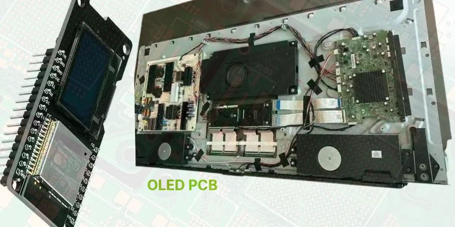
- A QD-OLED display PCB should be reviewed as a high-speed interface and power-control board for a self-emissive panel, not as a backlight board.
- The first engineering checks are panel interface choice, timing path, FPC and connector geometry, rail sequencing, thermal concentration around control ICs, and calibration access.
- QD-OLED modules remove the LCD backlight layer, but they still depend on careful PCB design for TCON, panel control, EMI containment, and bring-up stability.
- Most prototype failures come from interface mismatch, weak reference continuity, unstable rails, poor connector support, or treating panel calibration as a software-only issue.
- Early success usually depends on reviewing the panel architecture, flex routing, assembly tolerances, and debug path before the first prototype order is released.
QD-OLED combines a blue OLED light source with a quantum-dot conversion layer, so the PCB around the panel is mainly responsible for high-speed signal delivery, timing control, power behavior, thermal management, and production debug rather than backlight drive. The practical design question is whether the controller board can move clean video data and stable power into the panel without creating flicker, EMI, thermal stress, or bring-up ambiguity.
Contents
- What to review first on a QD-OLED display PCB
- Key design and validation rule table
- Early engineering trade-off table
- How interface and timing architecture affect layout
- How power, thermals, and HDR targets affect the board
- What prototype and assembly teams should freeze before release
- FAQ
- Next steps
- References
- Author and review
What to review first on a QD-OLED display PCB
QD-OLED is not the same as TFT-LCD with a different marketing label. According to Samsung Display's QD-OLED materials, the panel is a self-emissive structure built around a TFT layer, blue OLED emission, and a quantum-dot conversion layer. That means the supporting PCB does not need to solve a classic LED backlight problem, but it still has to solve high-speed panel interface, power integrity, thermal concentration, and calibration control.The first review points are usually:
- whether the target panel expects eDP, MIPI DSI, or another interface and whether the SoC or bridge really matches that requirement
- whether the timing and high-speed lanes can cross connectors and flex transitions with controlled return paths
- whether panel rails, logic rails, and any auxiliary power rails need controlled sequencing and fault handling
- whether heat from TCON, PMIC, bridge ICs, or nearby compute devices is being dumped into a mechanically constrained display area
- whether production and bring-up teams can still inspect, measure, and calibrate the module without disassembling the product
For compact display-control layouts, it is usually worth aligning the stackup with high-speed PCB and HDI PCB capability before layout freeze.
Key design and validation rule table
| Rule / parameter | What to check first | Why it matters | How to verify | If ignored | | --- | --- | --- | --- | --- | | Interface fit | Confirm the actual panel interface, lane count, and bridge requirements | QD-OLED module failure often starts with the wrong interface assumption, not with the panel itself | Panel documentation, controller datasheet, connector map review | No image, unstable link training, or late redesign | | Timing path | Treat the controller, flex, connector, and panel entry as one signal path | High-speed display behavior depends on the whole channel, not only the source IC | Layout review, [impedance calculator](/tools/impedance-calculator/) check, prototype scope plan | Flicker, noise, intermittent image loss | | Power sequencing | Review startup and shutdown order for logic and panel rails | Self-emissive displays still depend on predictable power behavior and control timing | Schematic review, bench bring-up checklist | Startup faults, latch-up risk, unstable image | | Thermal concentration | Map heat around TCON, PMIC, and nearby high-power components | Local heat can affect long-run stability and calibration consistency | Thermal review and prototype measurement plan | Hotspots, drift, shortened service margin | | Calibration and test access | Reserve access for rails, reset, interface debug, and image validation | Display tuning is slower and less repeatable without a defined test path | DFT review, test point review, pilot checklist | Long debug cycles and unclear root cause | | Mechanical and flex support | Freeze connector orientation, bend limits, and retention method | Many field failures start at flex and connector transitions | Mechanical review and first-article inspection | Intermittent faults or assembly damage |Early engineering trade-off table
| Design choice | Usually stronger for | Main trade-off | What to confirm early | | --- | --- | --- | --- | | eDP interface | Larger embedded displays, notebook-class or monitor-class panels | Cleaner ecosystem for many high-resolution embedded displays, but depends on panel support and link budget | Panel spec, lane budget, power-saving features | | MIPI DSI interface | Compact modules, mobile and automotive-oriented integration | Lower pin count and low EMI benefits, but routing and bridge compatibility can tighten quickly | D-PHY or C-PHY assumptions, bridge path, flex routing | | Integrated controller board | Tighter packaging and shorter signal path | More local thermal and EMI coupling | Enclosure space, thermal path, rework access | | Separate display control board | Easier partitioning and service access | Adds interconnect complexity and channel-loss risk | Cable length, connector count, grounding plan | | Conventional multilayer | Simpler fabrication on less dense control boards | Less escape freedom around fine-pitch interfaces | Package pitch, fanout density, outline limits | | HDI layout | Better for dense escapes and tighter flex transitions | Higher fabrication complexity and stronger stackup discipline required | Via strategy, build-up cost, yield path |How interface and timing architecture affect layout
The interface decision is usually the biggest design fork on a QD-OLED controller board. MIPI DSI is positioned by MIPI as a high-speed display interface for smartphones, tablets, laptops, automotive, and other embedded platforms, while VESA describes eDP as the de facto video standard for larger embedded displays, especially at 1080p and above.Three layout decisions usually determine whether the design is controllable.
1. Keep the channel continuous across controller, connector, and flex
The panel does not care whether loss or discontinuity came from the source IC breakout, the board connector, or the flex transition. If lanes neck down too hard, cross split references, or enter a connector with weak return support, the whole path becomes unstable. For denser control boards, HDI PCB routing often reduces compromise in the escape region.
2. Freeze the panel interface before mechanical packaging is locked
Late movement of connector orientation or flex fold direction often destroys a previously clean channel. If the product outline is still moving, the team should review the physical path in a Gerber viewer or PCB viewer before releasing fabrication data.
3. Match the debug plan to the real interface
Display debug should not begin with guesswork. Teams usually need defined access to reset, enable, reference clocks, rails, and interface activity. That matters more on QD-OLED builds because panel bring-up issues are often misdiagnosed as firmware problems when the physical path has not been proven first.
How power, thermals, and HDR targets affect the board
A QD-OLED panel is self-emissive, but the board around it still has to support stable power delivery and predictable thermal behavior. According to VESA's DisplayHDR criteria, HDR evaluation is not just about peak luminance. It also considers black level, active dimming behavior where relevant, color gamut coverage, and stability across multiple tests. In practical PCB work, that means the board has to support the panel and controller path consistently enough for the system target to be met, not just boot once on the bench.The main engineering checks are:
- separate sensitive logic and high-current conversion paths so noise does not bleed into timing or control signals
- confirm whether PMIC, bridge, and controller heat are trapped behind the panel or enclosure
- reserve measurement access for rail ramp, transient behavior, and image-state correlation
- align calibration expectations with manufacturing reality so brightness, color, and gamma validation are not left vague at pilot stage
If the board combines fine-pitch display control, dense routing, and tight mechanical packaging, turnkey assembly, SMT assembly, and PCB prototype planning usually needs to happen together rather than as disconnected handoffs.
What prototype and assembly teams should freeze before release
Prototype risk usually falls when the display board is released with both an electrical and a manufacturing plan, not just a schematic that looks complete.A practical release checklist usually includes:
- Panel and interface lock
Freeze the real target panel, interface family, lane expectations, and bridge assumptions before layout closure. - Stackup and channel review
Confirm controlled routing, connector transitions, and reference continuity for all critical display lanes. - Bring-up measurement plan
Decide where rails, reset, clocks, and interface activity will be checked on the first article. - Thermal review
Identify whether controller-side heat concentration needs spreading, shielding, or enclosure changes before pilot build. - Calibration and acceptance path
Define what image quality, startup behavior, and production inspection will count as acceptance for the prototype stage. - BOM and sourcing alignment
Use a BOM viewer review to catch connector, PMIC, bridge, oscillator, and panel-adjacent substitution risks before purchasing starts.
If the board is moving quickly into sample validation, quick-turn PCB support usually reduces avoidable delay between layout freeze and first power-on.
FAQ
Is a QD-OLED display PCB basically the same as an LCD backlight board?
No. QD-OLED is a self-emissive panel architecture, so the supporting PCB is mainly about signal delivery, timing, power behavior, thermal control, and calibration access rather than LED backlight driving.
Which interface is more common on QD-OLED modules, eDP or MIPI DSI?
It depends on product class and panel design. eDP is common on larger embedded displays, while MIPI DSI is common in compact embedded and mobile-oriented systems. The correct answer comes from the target panel and system architecture, not from a generic preference.
Does QD-OLED remove the need for careful thermal design?
No. Even without an LCD backlight board, the display controller path, PMICs, bridge ICs, and surrounding compute hardware can create local heat that affects stability and service margin.
Why is calibration planning part of PCB review?
Because brightness, color, gamma, and startup behavior cannot be validated efficiently if the board lacks stable rails, debug access, or a repeatable production test path.
When should HDI be considered for a QD-OLED controller board?
Usually when package escape is dense, connector geometry is tight, or the board needs cleaner routing around high-speed display lanes than a conventional breakout can provide.
Next steps
If you are building a QD-OLED product, the most useful next step is usually to review the interface path, rail sequencing, connector geometry, and thermal layout together before releasing the first prototype.HILPCB can support that process through:
- High-speed PCB planning for controlled display-channel routing
- HDI PCB support when package escape and connector density become the main bottlenecks
- SMT assembly and turnkey assembly coordination when fabrication and bring-up must stay aligned
- PCB prototype and quick-turn PCB for fast validation builds
- Impedance calculator, Gerber viewer, and PCB viewer for early channel and layout review
- Request a quote when your panel choice, stackup, and assembly package are ready