
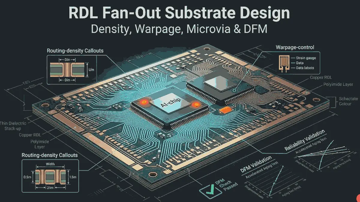
RDL fan-out substrates have become a critical structure in AI chips, chiplet packaging, and high-bandwidth interconnect platforms. For engineering teams, RDL fan-out substrate design is not just about making traces finer. It requires control of routing density, stack-up and power delivery, warpage behavior, microvia reliability, and the production process window at the same time. Many early-stage projects focus only on I/O fan-out count and channel density, but the risks that usually appear during pilot builds and validation are copper imbalance, overly aggressive microvia structures, excessive thermal mismatch, and manufacturing tolerances that were never converged early enough.
From a manufacturing-introduction perspective, the hardest part of RDL and fan-out substrate programs is not one local routing segment. The real challenge is whether ultra-fine lines, thin dielectrics, microvias, current density, and package assembly behavior can all be reproduced consistently under one process condition set. If structural design stays only at the simulation limit and is not aligned with the real process window, the penalty shows up later in warpage, cross-sections, reliability, or yield. A more reliable approach is to treat the RDL fan-out substrate as a system problem that combines design rules, manufacturing discipline, and a validation loop.
Why RDL Fan-Out Substrates Are Harder Than Standard High-Density Boards
Many teams think of an RDL fan-out substrate as just "finer HDI" or "a denser substrate," but the difficulty is not only the smaller geometry. Once interconnects move into fan-out packaging and high-bandwidth packaging, geometric margin, thermal margin, and reliability margin all become much tighter.
In real projects, the most common issues usually fall into four groups:
- Line width and spacing are pushed too close to the limit, so process variation quickly affects yield
- Power delivery and high-speed signals couple through thin dielectric layers, making SI and PI targets hard to satisfy at the same time
- Copper distribution and material combinations are unbalanced, creating warpage and assembly problems
- Microvia structures expose fatigue failure early under thermal cycling and assembly stress
Because of that, RDL fan-out substrates are not just a "high-density routing problem." They are a combined design, materials, manufacturing, and assembly problem.
Reference Table of Key RDL Fan-Out Substrate Design Parameters
The table below is not a fixed industry standard. It reflects common review windows used in RDL fan-out substrate projects. Final values still need to be confirmed according to package format, I/O scale, material system, and supplier capability.
| Parameter | Common Review Window | Design Note |
|---|---|---|
| Line width / spacing | Usually assessed from mature production capability rather than absolute limit | The ability to build it once does not mean it can be mass-produced consistently |
| Dielectric thickness | The thinner it gets, the more attention is needed on warpage and impedance variation | It should not be chosen only from routing density |
| Microvia strategy | Stacked, staggered, and filled-via options should be confirmed by use case | Reliability and production difficulty need to be judged together |
| Copper distribution | Both global and local copper balance need control | It directly affects lamination, warpage, and thermal behavior |
| Impedance and power delivery | High-speed channels and low-inductance power paths must both be satisfied | Teams cannot optimize only SI or only PI |
| Thermal boundary | Large compute die zones and HBM zones are usually the most sensitive | Thermal stress feeds back into microvia life |
| Panelization and assembly | Panel format and assembly temperature profile should be considered early | Die regions and local stress zones cannot be handled as an afterthought |
| Validation plan | Cross-sections, warpage, thermal cycling, and failure analysis should be defined early | It cannot wait until pilot-build failure |
If these parameters are not frozen before prototyping, teams usually end up repeating rework during the yield, warpage, and reliability stages.
Why Routing Density Must Be Built on a Stable Process Window
The first pressure point in RDL fan-out design is almost always I/O fan-out and routing density. AI chips and high-performance packaging need extremely high interconnect counts, which pushes designs toward finer lines, thinner dielectric layers, and more aggressive structures. But density by itself is not manufacturability.
During layout and DFM review, teams usually need to confirm first:
- Whether target line width and spacing are inside the supplier's repeatable production window rather than close to a one-time prototype limit
- Whether alignment tolerance in the tightest areas will consume the original design margin
- Whether capture pads, pads, and via structures still retain enough safety margin after manufacturing variation
- Whether this level of aggressive density is truly necessary once signals, power, and reference structures are reasonably partitioned
If the project is already approaching a more advanced interconnect window, teams can also reference advanced HDI manufacturing capability to understand why "possible once" and "stable in volume" are not the same thing.
Why Stack-Up, Power Delivery, and High-Speed Interconnect Must Be Evaluated Together
In fan-out substrates, separating signal integrity, power integrity, and mechanical structure usually leads to the wrong conclusion. The same stack-up defines channel impedance and loss, power-loop inductance, copper-balance behavior, and overall warpage at the same time.
A more reliable stack-up review usually confirms first:
- Whether high-speed channels need the support of high-speed PCB capability to control reference layers and the impedance window
- Whether the power structure really forms a practical low-inductance loop
- Whether copper balance is strong enough to support stable lamination and assembly
- Whether local thin-dielectric and high-density microvia regions remain compatible with the overall material behavior
- Whether the project is close enough to advanced packaging boundaries that IC substrate capability should be evaluated in parallel
Many stack-ups look ideal in simulation. But if they cannot balance power delivery, electro-thermal behavior, and warpage, they still become high-risk structures in production.
Why Warpage Control Must Start Before Layout Is Finished
In advanced packaging projects, warpage is not a problem for the back-end package stage alone. It directly affects placement yield, solder-ball connection, underfill behavior, and long-term reliability. Many teams spend nearly all of their early attention on routing density and impedance, only to discover after layout completion that local copper distribution and material selection have already locked in the warpage risk.
A more effective warpage review usually includes:
- Whether full-board copper symmetry is reasonable
- Whether there is local copper imbalance around large die zones, HBM zones, and power-dense regions
- Whether material thermal expansion and assembly temperature profile are compatible
- Whether substrate thickness, package size, and assembly path amplify local deformation
- Whether panelization and singulation method will change residual stress, which can be reviewed against the panelization design guide
If these issues are left until later stages, the fix is usually no longer a small parameter change. It often requires broader structural redesign.
Why Microvia Reliability Is a Core Gate for RDL Fan-Out Substrates
Microvias are a key enabler of RDL fan-out routing capability, but they are also one of the most common reliability risk sources. Stacked microvias, copper-fill quality, high aspect ratio, and thermal mismatch all turn into long-term failure risk under thermal cycling and assembly stress.
During design, teams should focus on confirming:
- Whether the project is better suited to stacked microvia or staggered microvia structures
- Whether the microvia aspect ratio is still inside a mature process window
- Whether copper fill and plating assumptions match the later production scale
- Whether local high-heat regions will amplify microvia fatigue
- Whether reliability targets have been written into the validation plan rather than left as layout assumptions
For AI chip interconnect platforms, passing one prototype build is not enough. What matters is whether the microvia structure can survive pilot production and long-term service conditions. For process-closure thinking, teams can also review AI chip interconnect MES traceability to understand why advanced packaging depends so heavily on production records.
Why Thermal Behavior and Current Density Must Be Judged Together
AI packaging power density is already high enough that thermal and electrical problems can no longer be treated as separate topics. The higher the current density, the higher the local temperature rise. The higher the temperature, the more material and interface behavior changes, which then accelerates fatigue in microvias, copper interfaces, and connection structures.
Thermal review usually needs to confirm first:
- Where the main current concentration zones and hot spots are
- Whether the power path forms a local thermal bottleneck
- How heat spreads through copper layers, dielectric material, and surrounding package structures
- Whether thermal-expansion mismatch is more severe in the hottest regions
- Whether thermal boundaries have already been passed into assembly and reliability validation
If the project also involves AI board-level interconnect introduction, teams can reference AI chip system background to understand why power density, thermal boundaries, and package interconnect are becoming harder to separate.
DFM Review and Production Validation Loop for RDL Fan-Out Substrates
Many teams think of RDL fan-out substrate validation as a qualification step after design is done. A more effective approach is to let DFM and validation logic constrain the design at the architecture stage. If stack-up, microvias, copper balance, and assembly path are not constrained by validation targets from the beginning, the modification cost is usually already high by the time failure analysis appears.
A practical production-validation path usually includes:
- Structural and process pre-review: Confirm that stack-up, line width and spacing, microvias, and copper distribution all stay inside a real process window.
- Warpage and assembly validation: Measure deformation and placement risk under representative assembly temperatures and process conditions.
- Thermal cycling and reliability validation: Include critical structures in the reliability test matrix.
- Cross-section and failure analysis: Build a first-article analysis loop for microvias, interfaces, and high-risk areas.
- Manufacturing handoff freeze: Use design handoff best practices to document process assumptions, material boundaries, and release conditions clearly.
If the project will later move into a more complex assembly path, teams can also review AI chip interconnect SMT challenges and turnkey PCBA introduction challenges to understand why fan-out substrate structural decisions still affect assembly yield.
Frequently Asked Questions About RDL Fan-Out Substrates
What is the biggest difference between an RDL fan-out substrate and a standard HDI board?
It is not just finer lines. The structure is constrained at the same time by ultra-fine interconnects, thin dielectrics, microvia reliability, warpage, and package assembly behavior. Variation that is acceptable on a normal HDI board is often amplified in a fan-out substrate.
Is higher density always better for an RDL fan-out substrate?
No. Density only matters when it sits inside a repeatable production window. Designs pushed too close to the limit usually pay a higher price in alignment, tolerance, and yield.
Why does the microvia strategy need to be locked early?
Because stacked vias, staggered vias, copper filling, and aspect ratio all affect routing capability, assembly window, and long-term reliability at the same time. If changes wait until after prototype failure, the redesign is usually much larger.
Why can't warpage be handled after layout is finished?
Because warpage is strongly tied to copper distribution, material combinations, and assembly path. Once layout is complete, the problem is usually beyond a local adjustment.
What should be frozen first before mass production?
First freeze the stack-up, line width and spacing window, microvia strategy, copper balance, assembly temperature path, validation matrix, and manufacturing handoff conditions. The later those are frozen, the larger the rework and pilot-build variation.
Conclusion
RDL fan-out substrate design is not just about pushing interconnects finer. It is about balancing routing density, power delivery, warpage control, microvia reliability, and production repeatability inside one structure. The most mature solution is usually not the most aggressive one on paper. It is the one that stays reliably inside a manufacturable, verifiable, and scalable window.
Next Steps
If your team is developing RDL fan-out substrates for AI chips, chiplets, or high-performance packaging, HILPCB can support with:
- Fan-out substrate structural pre-review: Identify line width, spacing, microvia, and copper-balance risks before fabrication -> See PCB manufacturing and DFM support
- High-speed and substrate capability coordination: Evaluate the right process path around interconnect density, power delivery, and material window -> See IC substrate capability
- Prototype introduction and reliability validation support: Connect warpage, thermal cycling, and failure analysis earlier -> Get a PCB fabrication and assembly quote
If you want to complete an RDL fan-out structural review, microvia reliability analysis, or DFM production-readiness check before the first build, contact the PCB engineering team to discuss the project.
Related Reading:
- Advanced HDI Manufacturing Capability: Why high-density interconnect structures must start from a real process window
- AI Chip System Background: How power, thermal behavior, and interconnect become tightly linked on high-compute platforms
- Reliability Test Matrix: Why advanced structures need an early validation plan
- AI Chip Interconnect MES Traceability: How to build a structural and failure-analysis loop in production
- Design Handoff Best Practices: How to write process assumptions and release conditions into delivery data