
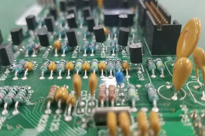
As automotive electronics moves rapidly toward intelligence and electrification, the architectures behind ADAS and EV systems are becoming more complex than ever—from ADAS domain controllers that process massive data, to BMS platforms managing hundreds of volts. Modern automotive PCBs carry safety-critical responsibilities, and mixed-technology designs (THT + SMT) create serious manufacturing challenges. In this context, Selective wave soldering emerges as a core process for meeting automotive-grade reliability and high-voltage safety requirements.
This article takes an automotive connectivity perspective to explain how Selective wave soldering supports ADAS and EV power PCB manufacturing, with emphasis on power integrity, high-speed signal paths, thermal reliability, and compliance with stringent automotive standards.
Core advantages of Selective Wave Soldering: why it’s the default choice for ADAS & EV PCBs
Traditional wave soldering can be disastrous for mixed-technology boards already populated with dense SMT devices, while pure hand soldering struggles to deliver the consistency and reliability required in automotive applications. Selective wave soldering solves this by using a small, precisely positioned solder nozzle to solder only the specified THT joints.
Key advantages include:
- High precision and repeatability: Automated control delivers consistent solder volume, dwell time, and temperature—critical for meeting ADAS radar PCB compliance.
- Minimized thermal stress: Heat is localized to the target area, protecting nearby sensitive SMT devices (SoC, PMIC, sensors) and avoiding secondary reflow damage.
- Excellent joint quality: With inert-gas protection (e.g., nitrogen), oxidation is reduced and bright, full, void-minimized joints are achieved—essential for long-term reliability in high-voltage/high-current environments.
- Design flexibility: Engineers can place THT and SMT on the same PCB and still achieve optimal electrical/mechanical performance—even in compact LiDAR interface board design layouts.
For automotive electronics, this controlled and reliable through-hole assembly process is a foundation for functional safety and product lifetime.
Domain-controller power distribution and high-voltage safety: the role of Selective wave soldering
In ADAS domain controllers and EV systems such as BMS or drive units, power integrity is a top priority. These systems often use high-current THT connectors, fuse holders, or busbars to carry tens to hundreds of amps.
Here, Selective wave soldering is a key enabler. Hand-soldered high-current connectors can vary by operator skill, leading to cold joints, insufficient solder, or weak fillets—latent failure points. Under high load, those defects raise contact resistance, create voltage drop, and generate Joule heating; in severe cases, connectors can overheat or fail dangerously. With tightly controlled solder flow, selective wave soldering forms full, uniform joints that fuse reliably with Heavy Copper PCB copper, reducing contact resistance and maximizing current-carrying capability.
For high-voltage systems, solder joint geometry also affects maintenance of clearance and creepage. Selective wave soldering reduces solder splash and minimizes icicles/spikes, producing smoother, controlled joint profiles aligned with HV safety requirements. When selecting BMS balancing board materials, compatibility with the soldering process also matters to maintain insulation performance and mechanical strength over long-term HV operation.
Process flow: Selective Wave Soldering steps
| Step | Core task | Key control points |
|---|---|---|
| 1. Fluxing | Apply flux precisely to target pins via micro-drop jetting or spraying. | Coverage area, flux volume, activity. |
| 2. Preheating | Heat from the PCB bottom side to activate flux and reduce thermal shock. | Preheat profile, heating uniformity. |
| 3. Soldering | A programmable mini-wave nozzle moves to each joint and solders precisely. | Solder temperature, nozzle type, dwell time, nitrogen protection. |
| 4. Cooling & Inspection | Cool in a controlled environment and inspect using AOI or X-Ray. | Cooling rate, joint appearance, internal voiding. |
High-speed SI challenges: soldering considerations for GMSL/FPD-Link and Ethernet interfaces
ADAS relies on cameras, radar, and LiDAR sensors, connected to domain controllers through high-speed serial interfaces such as GMSL, FPD-Link, and Automotive Ethernet, often at multi-Gbps rates. These interfaces are highly sensitive to impedance matching and SI.
In many designs, the external harness connector is a THT component. Inconsistent soldering introduces variable parasitic inductance/capacitance, leading to impedance mismatch, reflections, jitter, and eye closure—ultimately causing data errors. With its repeatable process control, Selective wave soldering keeps solder volume and fillet geometry highly consistent pin-to-pin, minimizing impact on differential impedance.
In dense LiDAR interface board design layouts, high-speed connectors may sit next to tightly packed SMT parts. Selective wave soldering’s precise positioning protects adjacent decoupling capacitors and filters while soldering the connector, preserving the end-to-end link. Surface finish selection—ENIG/ENEPIG/OSP—also matters for solderability and long-term reliability. ENIG/ENEPIG, with strong planarity and corrosion resistance, is often preferred for high-speed PCB.
Handling high-density layouts: coordinating VIPPO with the soldering process
To integrate more functions in limited space, automotive PCBs—especially ADAS modules—are increasingly built with HDI structures. Via-in-Pad plated over (VIPPO) places vias directly in pads and copper-fills/plates them flat, shortening signal paths and freeing routing space.
However, VIPPO can complicate soldering. In reflow or wave processes, solder can be wicked into vias, causing solder starvation and weak joints. Selective wave soldering helps here: a fast contact–solder–withdraw motion and precisely controlled solder volume reduce excessive wicking into VIPPO structures, ensuring reliable joints on the pad surface.
This coordination between Via-in-Pad plated over (VIPPO) and selective wave soldering makes it feasible to place THT connectors even in extremely compact designs (e.g., palm-sized camera modules) without sacrificing electrical performance or reliability. HILPCB has extensive experience with complex HDI PCB builds and can integrate advanced fabrication with precise assembly processes.
HILPCB capability highlights
- ✅ Process expertise: Selective wave soldering, PoP (Package on Package) assembly, BGA rework and reballing.
- ✅ Technical support: Via-in-Pad plated over (VIPPO), Back-drilling, and blind/buried via HDI structures.
- ✅ Materials & surface finishes: Multiple BMS balancing board materials options and ENIG/ENEPIG/OSP processes.
- ✅ Quality system: IATF 16949-aligned automotive quality management to meet automotive-grade requirements.
Thermal management and reliability: from SoC/PMIC to BMS
Automotive electronics operate in harsh environments with large temperature swings (-40°C to 125°C), continuous vibration, and mechanical shock. Thermo-mechanical reliability of solder joints often defines product lifetime.
THT components (large electrolytic capacitors, power inductors, connectors) are heavier and see higher mechanical stress under vibration. A high-quality solder joint is not only an electrical connection—it is also mechanical support. The full, uniform fillet formed by Selective wave soldering helps distribute stress and reduces crack risk.
From a thermal perspective, these THT parts can be significant heat sources. A solid, void-minimized joint provides a good heat path, transferring heat into PCB copper for spreading. This supports stable SoC/PMIC operation and helps extend the life of BMS balancing board materials. With strict process control, selective wave soldering can meet IPC-A-610 Class 3 joint quality, a baseline requirement for ADAS radar PCB compliance.
Surface finish vs. solder quality: ENIG/ENEPIG/OSP selection and impact
Surface finish directly affects solderability and long-term reliability on mixed-technology assemblies.
- OSP (Organic Solderability Preservatives): lower cost and very flat for SMT, but weaker thermal robustness; solderability may drop after multiple thermal cycles (SMT reflow + selective wave), requiring a tighter process window.
- ENIG (Electroless Nickel Immersion Gold): strong planarity, good solderability, and long shelf life; commonly used in automotive because it tolerates multiple thermal cycles well.
- ENEPIG (Electroless Nickel Electroless Palladium Immersion Gold): adds a Pd layer to reduce Black Pad risk and improve wire-bond reliability; often chosen for the highest reliability modules (airbag controllers, ADAS core units).
In Selective wave soldering, ENIG/ENEPIG often provide the most stable soldering behavior, enabling reliable IMC formation. Choosing the right ENIG/ENEPIG/OSP is a first step toward reliable LiDAR interface board design and other critical automotive electronics.
HILPCB assembly service advantages
- One-stop delivery: From PCB fabrication to component sourcing, SMT and THT soldering, we provide full turnkey assembly to simplify your supply chain.
- Advanced equipment: Top-tier selective wave soldering equipment with nitrogen protection for exceptional joint quality.
- Engineering support: Our DFM/DFA engineers engage early to optimize manufacturability and reliability.
- Flexible capacity: Fast prototypes to low/mid-volume production—delivered efficiently to accelerate time-to-market.
Conclusion: building the future of automotive electronics with process excellence
As automotive electronics moves toward higher integration, higher performance, and higher safety, manufacturing process evolution becomes a core driver. It is no longer just a way to connect components—it is a key technology that determines final performance, reliability, and safety. From stabilizing ADAS domain-controller power delivery, to protecting GMSL SI, to handling HDI challenges, Selective wave soldering demonstrates its unique value.
By combining advanced PCB fabrication (such as Via-in-Pad plated over (VIPPO)) with precise assembly, and by selecting the right BMS balancing board materials and ENIG/ENEPIG/OSP surface finish, HILPCB is committed to delivering electronics manufacturing that meets the most demanding automotive standards. We know every perfect solder joint is a serious safety commitment. Choosing HILPCB means choosing a partner that understands and can execute the complexity of automotive electronics—building reliable mobility through excellent Selective wave soldering.
Common Questions
Why is selective wave soldering important in automotive ADAS and EV power electronics?
These products often use heavy through-hole connectors, inductors, relays, and power parts that must survive vibration, temperature cycling, and long service life. Selective wave soldering improves repeatability and helps deliver joints suited to automotive reliability expectations.
Can solder joint quality affect high-speed automotive interfaces?
Yes. Connectors carrying GMSL, FPD-Link, or automotive Ethernet signals are sensitive to parasitic variation. Inconsistent solder geometry can disturb impedance and signal integrity, especially as interface speeds continue to rise.
Why do surface finish choices matter for automotive selective soldering?
Finishes such as OSP, ENIG, and ENEPIG influence solderability, process window, and long-term corrosion resistance. Automotive programs usually need a finish choice that supports both assembly repeatability and long service reliability.
What should teams validate before releasing an automotive selective-solder process?
They should verify joint consistency, thermal behavior, inspection coverage, and performance under realistic electrical and environmental conditions. In safety-related electronics, assembly quality has to be treated as part of the overall system risk.