
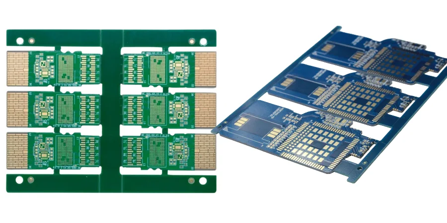
As data centers evolve toward 800G and beyond, optical modules—the core of electro-optical conversion—are growing exponentially in PCB design and manufacturing complexity. As a reliability and compliance engineer focused on GR-468/IEC compliance, I know every manufacturing step matters to long-term stable operation. Among them, Selective wave soldering is a key process for solving soldering challenges on high-density mixed-technology PCBs (SMT + THT). It is not just “a soldering method”; it is a precision engineering discipline that balances thermal stress, SI, and mechanical strength—directly shaping final optical-module performance and reliability.
This article focuses on Selective wave soldering in data-center optical-module PCB manufacturing: where it fits, what can go wrong, and how to optimize it. Starting from GR-468 reliability requirements, we examine how this process affects thermal management and high-speed signaling, and we connect materials science, process control, and failure analysis to show what it takes to build high-performance optical-module PCBs that pass strict standards.
Selective wave soldering fundamentals and applications in optical-module manufacturing
Selective wave soldering is an automated soldering process designed for mixed-technology boards. Unlike traditional wave soldering that immerses an entire PCB into a solder wave, it uses one or more mini nozzles to deliver molten solder precisely to targeted Through-Hole Technology (THT) pins. The overall flow includes three key steps:
- Precise flux application: Apply flux only where soldering is needed to avoid contaminating adjacent SMT components.
- Localized preheating: Preheat the soldering region to activate flux and reduce thermal shock.
- Mini-wave soldering: Use a precisely controlled solder nozzle to solder one or multiple pins quickly and reliably.
In optical modules—especially during OSFP 800G transceiver board manufacturing—PCBs integrate dense SMT devices (DSP, drivers, TIA) along with critical THT parts (high-frequency connectors, power interfaces). Full-board wave soldering can damage temperature-sensitive SMT parts, while manual soldering suffers from poor consistency and low reliability. Therefore, Selective wave soldering becomes the only practical automated solution: it delivers mechanical strength and electrical reliability for THT connectors while protecting sensitive neighboring parts. It is a cornerstone for high-quality Through-hole Assembly.
Under GR-468/IEC, selective wave soldering reliability validation and key challenges
Telcordia GR-468-CORE is the well-known “reliability bible” of the optical-communications industry. It defines harsh environmental and mechanical stress tests to simulate extreme real-world conditions for optical modules. For Selective wave soldering, solder-joint quality directly affects whether a module can pass key tests such as:
- Temperature Cycling: GR-468 requires hundreds to thousands of cycles from -40°C to +85°C. Residual stress induced during selective soldering—if not controlled—can be amplified by CTE mismatch during cycling, leading to solder fatigue cracks or pad lift.
- Damp Heat: Long exposure at 85°C/85%RH tests corrosion resistance and flux-residue inertness. Dirty soldering or overly active flux residues can trigger electrochemical migration and short failures.
- Mechanical Shock and Vibration: Simulates mechanical stress during transport and handling. Selective wave soldering must form full, robust joints so large THT connectors remain secure under vibration.
In practice, a small oversight at any point can surface in the final QSFP-DD module PCB testing stage, causing expensive rework or even scrapping entire lots. Therefore, GR-468 requirements must be embedded into process development from day one, using strict Process Validation and ongoing SPC to ensure long-term solder-joint reliability.
🛡️ Selective wave soldering: GR-468 high-reliability compliance workflow
For harsh telecom and optoelectronics environments, use a closed-loop THT process to target zero failures across the full lifecycle.
Evaluate THT pin spacing and SMT keep-out for heat; optimize the dedicated soldering pallet structure to prevent secondary thermal shock during selective soldering.
Select GR-468-compliant, oxidation-resistant SAC305 alloy and ultra-low-residue flux; match PCB surface finishes compatible with high-frequency materials (e.g., ENEPIG) to suppress whisker growth.
Build multi-dimensional DOE experiments to precisely define preheat slope, dwell time, and nozzle N2 flow; ensure Hole Fill > 75% as an industrial upper-bound target.
Run 3D X-Ray voiding checks and IC (Ion Chromatography) tests to control contamination levels and ensure electrochemical stability for downstream electro-optical signal transmission.
Run core stress tests such as Damp Heat (85/85) and Thermal Cycling to validate solder-joint structural strength under extreme mechanical stress and temperature/humidity load.
Capture solder-wave dynamics and wave-motor frequency in real time; introduce Cp/Cpk monitoring for minute-level early warnings against process drift, locking in batch consistency.
Thermal-stress management: the dual impact of selective wave soldering on high-speed SI
In high-speed digital circuits, SI is the lifeline. For a data-center Laser driver PCB, data rates can reach 112 Gbps/lane; even tiny impedance fluctuations can severely distort signals. Selective wave soldering is a localized high-temperature process, and its thermal effect has a dual impact on SI.
On one hand, it introduces risk. Instantaneous temperatures above 260°C can heat the PCB and cause temporary or permanent changes to local Dk/Df. This directly affects Controlled impedance, creates discontinuities, and leads to reflections and jitter—especially for high-speed differential pairs near THT connectors.
On the other hand, with precise control we can minimize the impact. This requires:
- Optimize the preheat profile: Sufficient and uniform preheating reduces ΔT and lowers thermal shock to the laminate.
- Shorten solder contact time: While ensuring good wetting, minimize nozzle-to-pad contact time to limit heat diffusion range and depth.
- Use high-performance laminates: Choose materials with higher Tg and low Z-axis CTE, such as Megtron 6 or Tachyon 100G. These High-Speed PCB materials maintain electrical and mechanical stability better at elevated temperature, protecting Controlled impedance consistency.
As reliability engineers, we must collaborate closely with design and manufacturing teams, using Thermal Simulation and empirical testing to find the best balance between process parameters and material behavior—so we achieve reliable mechanical interconnects without sacrificing SI.
Materials and surface finish co-optimization: choosing ENIG/ENEPIG/OSP
Surface finish is the bridge between components and the PCB, and its selection directly impacts Selective wave soldering results and long-term solder-joint reliability. In optical-module manufacturing, common finishes include ENIG/ENEPIG/OSP.
- ENIG: Excellent planarity and solderability, commonly used for high-speed PCBs. However, multiple thermal cycles in selective soldering may increase Black Pad risk (over-corroded nickel leading to brittle joints). This requires strict control of plating-bath stability and gold thickness.
- ENEPIG: Adds a palladium layer between nickel and gold, reducing nickel migration/oxidation and improving solder-joint reliability—especially for complex HDI PCB designs that see multiple soldering cycles. While more expensive, reliability gains can justify it in high-end OSFP 800G transceiver board manufacturing.
- OSP: Low cost and eco-friendly with very flat surfaces. However, OSP films can decompose at high temperature. In complex flows that include multiple reflows plus selective soldering, protection can degrade, leading to THT pad oxidation and soldering defects.
Therefore, finish selection is a system decision that must weigh cost, signal performance, assembly complexity, and reliability goals. For high-performance optical modules, ENEPIG is often the best overall choice for performance + reliability, while ENIG provides a solid balance between cost and performance. At HILPCB, we provide materials and surface-finish consultation to ensure your Selective wave soldering success starts at the source.
HILPCB capability: precision process assurance
| Process parameter | HILPCB control standard | Reliability impact |
|---|---|---|
| Solder temperature control | ±2°C | Prevent heat damage and keep IMC thickness uniform |
| Solder contact time | Controlled to 0.1 s | Avoid overheating, control IMC growth, prevent laminate delamination |
| N2 protection | Purity >99.99%, O2 <20 ppm | Reduce oxidation, improve wetting, and form bright, reliable joints |
| Pallet material | Durostone® or equivalent ESD composite | Ensure accurate positioning, protect SMT components, prevent PCB deformation |
Process parameter optimization and defect prevention: long-term reliability via the Arrhenius model
Ultimately, Selective wave soldering success depends on tight control of key parameters: preheat temperature, flux volume, solder temperature, wave height, and soldering time. Any drift can cause common defects such as:
- Bridging: Solder connects adjacent pins, often due to insufficient flux activity or incorrect separation speed after soldering.
- Solder Skips: Solder fails to wet pads/pins, typically due to oxidation, insufficient flux coverage, or inadequate preheat.
- Icicles: Sharp protrusions form on joints and reduce electrical clearance.
- Thermal Shock: Excessive ramp rate creates internal stress in components or laminate, inducing micro-cracks.
From a reliability-engineering perspective, visible defects are only the tip of the iceberg. A deeper risk is lifetime reduction caused by thermal exposure. According to the Arrhenius model, aging rate increases exponentially with temperature. Localized high temperatures in selective soldering accelerate IMC growth inside solder joints. While an appropriate IMC layer is required for metallurgical bonding, overly thick or non-uniform IMC becomes brittle and can significantly reduce fatigue and shock resistance—shortening product life in the field.
Therefore, the goal is to find a process window that forms robust joints while minimizing thermal aging. This often requires methods such as HALT and HASS to proactively expose weaknesses early in development, then optimize accordingly—so products like data-center Laser driver PCB can meet multi-decade design-life expectations.
Consistency testing and failure analysis: securing mass-production quality for QSFP-DD modules
Even after parameters are optimized, consistency in mass production remains challenging. For high-value optical modules, robust test and failure-analysis flows are the last line of defense. QSFP-DD module PCB testing is a system engineering effort that spans the assembly lifecycle.
After Selective wave soldering, we immediately use AOI and X-Ray to check external joint shape and internal structure (voiding, wetting, etc.). But that is not enough. Functional and reliability validation is equally important:
- ICT / flying probe: Verify electrical continuity for THT connectors and ensure no opens/shorts.
- FCT: Test assembled PCBs in a simulated operating environment to verify electro-optical conversion function and signal quality.
- Stress Screening: Run short temperature cycling or random vibration on some or all products to screen out early “infant mortality” units.
If failures are found, an efficient failure-analysis (FA) flow is critical. We use SEM, EDX, solder cross-sections, and other tools to pinpoint root causes. For example, a connector that fails vibration testing may show overly thick IMC in cross-section, traceable to excessive selective-solder contact time or overly high temperature. This closed-loop from test → analysis → process improvement is essential to ensure QSFP-DD module PCB testing pass rate and final product quality. HILPCB’s Turnkey Assembly includes such a complete QC and traceability system.
Assembly advantages: HILPCB’s end-to-end reliability assurance
- Expert-level DFM/DFA analysis: Engage early in design to optimize selective-solder process window and avoid common design traps.
- Advanced equipment and environment: Use industry-leading selective wave soldering equipment with N2 protection, and assemble in a Class 100,000 cleanroom to eliminate contamination.
- Comprehensive process monitoring: Monitor all critical parameters in real time and maintain a traceable database so every PCB build has evidence.
- One-stop testing solutions: Provide end-to-end services from AOI/X-Ray to ICT/FCT and full GR-468 reliability testing to accelerate time-to-market.
- Fast-response FA team: Experienced FA engineers and complete analysis equipment enable quick root-cause identification and actionable CAPA.
HILPCB reliability engineering practice: end-to-end assurance from design to validation
At HILPCB, we are not only a PCB manufacturer and assembly provider—we also act as a reliability engineering partner. We understand that Selective wave soldering success is not an isolated operation; it is a system engineering discipline across the lifecycle.
Our service starts at design. Our DFM engineers co-review designs to ensure adequate clearance around THT components, compliant pad design, and fixture space for soldering pallets. Based on your application and reliability targets, we recommend appropriate base materials (e.g., Rogers PCB) and surface finish (e.g., ENIG/ENEPIG/OSP), and we run precise Controlled impedance modeling and simulation.
During fabrication and assembly, we execute the process controls and test standards described above. Whether your product is a complex OSFP 800G transceiver board manufacturing program or a cost-sensitive data-center Laser driver PCB, we tailor solutions to optimize the quality/cost balance.
Finally, we provide detailed consistency-test and reliability-evaluation reports as evidence of GR-468/IEC compliance. The goal is to build reliability into your product through disciplined engineering—not merely “filter” via testing.
Common Questions
Why is selective wave soldering so important for data-center optical modules?
Optical modules combine fine-pitch structures, sensitive materials, and strict reliability targets, so uncontrolled hand or bulk soldering adds too much thermal and dimensional risk. Selective wave soldering gives tighter heat input and better repeatability for connector and through-hole regions that still need robust joints.
What should engineers watch when balancing reliability and thermal stress?
They need to control preheat, solder contact time, nitrogen environment, and surface-finish compatibility so joints form properly without accelerating IMC growth or laminate damage. The goal is not only a good-looking joint, but one that survives field vibration, humidity, and thermal cycling over time.
Why are failure analysis and consistency testing necessary after process optimization?
A tuned recipe is not enough if mass production drifts. Consistency testing, AOI/X-Ray, FCT, and structured FA close the loop between observed failures and process settings, which is how long-life optical-module quality is maintained at scale.
Conclusion
Selective wave soldering is an indispensable precision process in modern data-center optical-module manufacturing. It directly determines mechanical strength, electrical performance, and long-term reliability. To truly master it requires system thinking across design, materials, process, and testing—and a deep understanding of their interactions.
As a reliability and compliance engineer, I believe only by strictly following standards like GR-468, understanding the complex interplay among thermal stress, SI, and materials science, and enforcing rigorous process control and validation can you deliver high-performance optical modules that run reliably for decades in harsh data-center environments. At HILPCB, we put these principles into practice with strong engineering capability and zero compromise on quality—helping customers win in competitive markets. Mastering Selective wave soldering means holding the key to high-reliability optical-module manufacturing.