
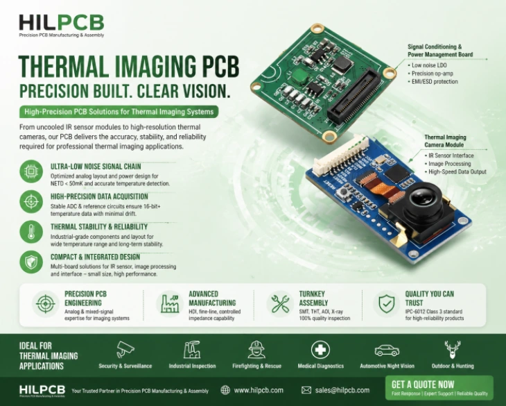
The global thermal imaging market reached $4.7 billion in 2023, with defense and security applications accounting for over 45% of revenue. Thermal imaging systems detect infrared radiation emitted by objects based on their temperature, producing images where warmer objects appear brighter than cooler surroundings. The PCB electronics perform three critical functions: biasing and reading out the infrared focal plane array (FPA), driving the cryogenic cooler, and processing raw detector output into a calibrated thermal image.
Thermal imaging development is concentrated in the United States (FLIR/Teledyne, L3Harris, Raytheon), France (Thales, Safran), the United Kingdom (Leonardo), and Germany (Hensoldt). These companies drive demand for thermal imaging PCBs combining ultra-low-noise analog performance with military-grade environmental qualification.
The performance metric defining a thermal imaging system is NETD—Noise Equivalent Temperature Difference—the smallest detectable temperature change. While fundamentally limited by detector physics, PCB-induced noise directly degrades achieved NETD. A well-designed board achieves detector-limited NETD; a poorly designed one degrades it by 2–5×.
HILPCB Manufacturing Capability: We fabricate thermal imaging PCBs with ultra-low-noise analog layout, isolated cooler driver sections, heavy copper for Stirling motor drivers, and rigid-flex configurations for compact camera assemblies—meeting IPC-6012 Class 3 for defense and industrial programs.
In This Guide
- Infrared Detector Technologies and PCB Implications
- Focal Plane Array Readout Circuit Design
- Cryogenic Cooler Driver and NETD Optimization
- Image Processing, Video Output, and Display
- Construction, DFM, and Production Testing
- HILPCB Thermal Imaging PCB Manufacturing
Infrared Detector Technologies and PCB Implications
The choice between cooled and uncooled technology determines fundamental PCB architecture—power budget, noise sensitivity, mechanical construction, and cost. Each creates distinct board-level challenges that must be addressed from earliest layout planning.InSb and HgCdTe photon detectors operate at 77–150 K, requiring a Stirling or pulse-tube cryocooler, extremely stable bias voltages (drift <10 μV per integration period), and high-speed ROIC readout at 30–120 Hz with 14–16 bit depth. VOx or a-Si microbolometers operate at room temperature with TEC stabilization (25 ± 0.1°C), <0.01% bias current stability, and higher-gain preamplifiers.
| Parameter | Cooled (InSb/HgCdTe) | Uncooled (VOx Bolometer) |
|---|---|---|
| NETD | 15–25 mK | 40–60 mK |
| PCB power | 5–15 W (mostly cooler) | 1–3 W |
| Readout speed | 10–120 MHz pixel clock | 5–30 MHz pixel clock |
| Noise sensitivity | Critical (detector-limited) | High (bolometer masks PCB noise) |
| Board cost | $200–500 (rigid-flex HDI) | <$10–50 (4–6 layer FR-4) |
Focal Plane Array Readout Circuit Design
The FPA readout conditions raw detector output for digitization. Whether cooled or uncooled, the board must achieve noise floors preserving the detector's intrinsic NETD—making layout and grounding the most critical design aspects.The signal chain includes transimpedance amplifier at ROIC output, correlated double sampling (CDS) for kTC noise removal, programmable gain amplifier, and 14–16 bit ADC at the pixel clock rate. The preamplifier's >10 MΩ input impedance makes it sensitive to capacitive coupling from switching signals.
Achieving Detector-Limited Performance
- Stripline Shielding: Analog signals on dedicated multilayer stripline layers between continuous ground planes.
- Digital Separation: No digital traces within 3 mm of the preamplifier input; orthogonal crossing where unavoidable.
- Star-Point Grounding: Analog-to-digital ground connection at a single location preventing switching current from flowing through the measurement path.
- Local Bypass: Capacitors on every analog supply pin within 2 mm of the load.
- Clock Precision: ADC sampling clock jitter below 5 ps RMS for 14-bit accuracy at 60 MHz, using differential LVPECL or LVDS distribution on inner stripline layers.
Cryogenic Cooler Driver and NETD Optimization
The cooler driver is simultaneously the highest-power and highest-noise PCB section. Managing its electrical noise while delivering sufficient drive current is the central challenge in thermal imaging board design—and the primary reason many cameras fail to achieve detector-limited NETD.Stirling cryocoolers use a linear motor at 40–80 Hz with 2–5 A peak current. The PCB provides sinusoidal drive (H-bridge PWM with LC filter), temperature sensing, position feedback, and protection. The PWM frequency (20–50 kHz) and harmonics couple into the readout, degrading NETD.
At HILPCB, our cooler driver isolation addresses this through reinforcing techniques:
- Separate Ground Region: Cooler driver on its own ground plane connected to main ground at a single point.
- Heavy Copper Motor Traces: 2 oz copper reduces I²R heating and thermal gradients near the detector.
- LC Power Filtering: Multi-stage filtering attenuates conducted noise >60 dB at PWM fundamental.
- Spread-Spectrum PWM: Distributes switching energy across wider bandwidth, reducing peak harmonic density.
NETD is degraded by three PCB sources addressed through coordinated stack-up design: power supply ripple (multi-stage LC filters within 2 mm of load pins), digital switching noise (minimum 5 mm separation from analog paths), and cooler drive harmonics (separate board section with single-point ground).
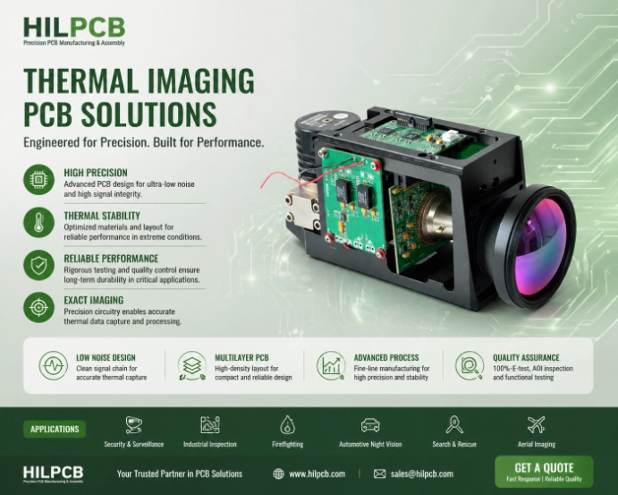
Image Processing, Video Output, and Display
Beyond readout, the PCB performs real-time NUC (non-uniformity correction), image enhancement, multi-format video output, and lens motor control—digital processing functions generating significant noise that must be isolated from the analog front end.Each FPA pixel has different responsivity and offset. NUC subtracts stored offset maps and applies gain correction at frame rate (1–4 MB calibration data per reference point). The processing FPGA or ISP with BGA packaging adds contrast optimization, digital zoom (2×–8×), target tracking, and video formatting. DDR memory frame buffers and high-speed video output interfaces require controlled impedance routing that must coexist with the low-noise analog section.
Defense cameras output multiple formats: analog PAL/NTSC, RS-170/STANAG 3350, HDMI/SDI, and GigE/USB3 Vision. Motorized zoom/focus lenses draw 200–500 mA requiring dedicated motor drivers with isolated supply filtering and ground return paths. Field-deployable cameras benefit from modular board architecture—separate detector, processing, and power boards connected by board-to-board connectors for independent module replacement.
Construction, DFM, and Production Testing
Handheld thermal cameras and weapon sights use rigid-flex construction connecting detector interface, processing, and display driver through flex sections folding within the housing—eliminating connectors and reducing weight 20–30%. Gimbal-mounted airborne systems use dynamic flex rated for >100,000 bend cycles. Assembly follows a specific sequence: populate the largest rigid section, fold to the next section, populate, repeat—verifying continuity after each fold.Production noise verification uses bench fixtures applying reference signals to measure the analog chain noise floor—boards exceeding the NETD budget are rejected. Cooled IR detectors demand ISO 7+ cleanroom conditions for the final detector-to-PCB connection, with ionic contamination below 1.56 μg/cm² per IPC-TM-650.
The Stirling driver requires MIL-STD-461G CE102/RE102 EMI compliance. Thermal cameras undergo continuous cycling between ambient and operating state—MIL-STD-810H Method 503 validates solder joint reliability over 500+ cycles.
Why Thermal Imaging OEMs Choose HILPCB
HILPCB serves thermal imaging manufacturers across the United States, France, Germany, and the United Kingdom. Our capabilities address cooled and uncooled product lines: low-CTE materials and rigid-flex for cryogenic proximity boards, precision analog routing and HDI packaging for compact microbolometer products spanning building inspection through automotive night vision.
Every board ships with IPC-6012 Class 3 certification, conformal coating compatibility, and SMT assembly with process controls for defense thermal imaging programs. From prototyping through production, our DFM review addresses noise isolation, cooler driver EMI containment, and rigid-flex assembly sequencing.
Thermal Imaging PCB FAQ
How does PCB noise impact the NETD of a thermal camera?
Noise Equivalent Temperature Difference (NETD) defines a camera's thermal sensitivity. If the PCB injects electrical noise into the focal plane array (FPA) readout—via power supply ripple, digital crosstalk, or cooler driver harmonics—it masks minute temperature differences, severely degrading the camera's effective NETD.
Why is the cryogenic cooler driver the biggest challenge in thermal PCB design?
Cooled MWIR/LWIR detectors require Stirling cryocoolers driven by linear motors drawing heavy, pulsed currents. This generates intense EMI. The PCB must isolate this noise using dedicated ground planes, spread-spectrum PWM, and heavy copper traces, preventing the harmonics from coupling into the ultra-sensitive microvolt-level detector readout.
Why are rigid-flex PCBs commonly used in handheld thermal imagers?
Military weapon sights and handheld FLIR cameras have severe space and weight constraints. A rigid-flex PCB integrates the detector readout, processing, and display driver onto a single foldable assembly, eliminating bulky connectors, reducing weight by 20-30%, and improving overall mechanical reliability against recoil shock.