
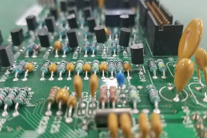
Through-hole technology looks old only when it is discussed without context. In 5G Advanced radio units, microwave test hardware, timing boards, power-interface modules, RF front ends and early 6G or sub-THz prototypes, THT through-hole soldering is still used where mechanical strength, current handling, connector retention, shielding, and service durability matter more than component density.
That does not mean through-hole soldering belongs everywhere. Small-signal RF paths, mmWave launch structures, dense DSP/FPGA regions and high-speed serial links usually prefer surface-mount, HDI, controlled-impedance routing and carefully designed board-to-package transitions. The useful engineering question is narrower: where does THT still create the strongest manufacturing outcome, and how should its parasitics, heat cycles and inspection plan be controlled so it does not damage RF performance?
This guide explains how HILPCB reviews THT and mixed-assembly communication PCBs for 5G, O-RAN radio hardware, mmWave modules and 6G research platforms. It covers RF connectors, cavity filters, power terminals, shield cans, selective wave soldering, low-void BGA reflow, ICT/FCT fixture planning, RF de-embedding and MES traceability.
Key takeaways
- THT is not a default high-frequency choice. It is a targeted assembly method for connectors, high-power interfaces, shield structures, bulky passives, filters and mechanically stressed parts.
- On RF communication boards, through-hole leads, barrels, solder fillets and ground returns can change impedance, insertion loss, return loss and out-of-band behavior.
- Mixed SMT + THT assembly must be planned as a thermal process. A second soldering step can stress BGAs, crystals, oscillators, RF modules and sensitive passives.
- Selective wave soldering, fixture design, inspection criteria and MES traceability are often more important than the soldering method name itself.
- A through-hole solder joint can support a 5G or 6G communication product, but it does not prove RF compliance, O-RAN interoperability, 6G readiness or field reliability by itself.
In this guide
- Where THT still belongs in 5G and 6G communication hardware
- THT versus SMT for RF, power and mechanical functions
- RF parasitics: what through-hole soldering changes electrically
- Mixed SMT and THT assembly: thermal shock, BGA risk and process order
- Selective wave soldering, inspection and acceptance control
- RF fixture design, de-embedding and production correlation
- Traceability/MES for communication PCBA manufacturing
- Common failure modes
- Cost drivers
- RFQ checklist
- Reference standards and engineering boundaries
- FAQ
Where THT still belongs in 5G and 6G communication hardware
5G Advanced and future 6G research hardware use many board types. A single system can include radio-unit RF boards, baseband cards, clock distribution boards, fronthaul interface boards, power modules, phased-array antenna assemblies, test fixtures and thermal interface hardware. These boards do not all need the same assembly method.
THT through-hole soldering remains valuable when the part is exposed to force, heat, high current or repeated service handling. The common examples are RF coaxial connectors, power-entry terminals, board-edge interfaces, large inductors, shield-can anchors, press-fit or soldered pin headers, some cavity filters, high-power passives and ruggedized I/O connectors. In these cases, the plated hole and solder fillet provide mechanical load sharing that a small SMT pad may not tolerate well under torque, cable pull, vibration or field maintenance.
For dense high-speed logic, the tradeoff changes. DSPs, FPGAs, retimers, Ethernet PHYs, clock buffers and memory devices are normally SMT or BGA components because the routing density and signal speeds demand short interconnects. That part of the board belongs to SMT assembly, HDI PCB and high-speed PCB review rather than to a through-hole-first decision.
The boundary is especially important in mmWave and 6G research boards. Terms such as 5G Advanced, sub-THz, lower THz, eCPRI, O-RAN, beamforming and timing synchronization describe the system context. They do not mean every interconnect on the PCB can be treated as a microwave transmission path. Some THT joints are outside the RF-critical path and mainly serve mechanical or power functions. Others sit close enough to RF launches, filters or cavity structures that their solder geometry must be treated as part of the RF design.
A good communication PCBA review therefore starts with a simple classification:
| THT location | Typical parts | Main reason for THT | What must be controlled |
|---|---|---|---|
| RF connector area | N-type, 4.3-10, SMA, SMPM, test connectors | Retention force, ground continuity, field service durability | Launch geometry, ground via fence, solder fill, connector coplanarity, torque stress |
| Filter or resonator area | Cavity filters, high-Q inductors, bulky RF passives | Mechanical support and designed package interface | Lead length, ground inductance, shielding, coupling to nearby RF nets |
| Power-entry area | DC input terminals, bus connectors, high-current pins | Current capacity and mechanical strength | Copper weight, hole plating, solder fill, thermal relief, creepage/clearance |
| Shield and chassis area | Shield-can tabs, grounding posts, mechanical anchors | EMI containment and chassis bonding | Ground path inductance, solder wetting, coating keepout, rework access |
| Test and service area | Pin headers, programming connectors, coax test points | Repeatable debug or production test access | Probe durability, mechanical strain, isolation from RF-sensitive nodes |
The design decision is not “THT or SMT.” It is “which joint is carrying which job?” Once that job is clear, the DFM, inspection and test strategy become much more precise.
THT versus SMT for RF, power and mechanical functions
SMT wins on miniaturization, automation, shorter parasitic paths and dense routing. THT wins where mechanical strength, thermal mass, high-current entry, service torque or ruggedized retention dominate. Most 5G and 6G communication PCBAs use both.
| Review item | THT through-hole soldering | SMT assembly |
|---|---|---|
| Mechanical strength | Strong for connectors, terminals, filters and heavy parts because leads pass through the board | Strong for small components, but large/heavy parts can stress pads under vibration or cable load |
| RF parasitics | Lead length and barrel geometry can add inductance/capacitance; must be modeled near RF paths | Usually lower parasitic length for chip components and high-speed packages |
| Routing density | Consumes space on multiple layers and may block routing channels | Supports high density, fine pitch and BGA routing |
| Thermal behavior | Can create a useful vertical heat path for some power or ground structures | Depends on pad area, thermal vias, planes and package design |
| Process complexity | Requires wave, selective wave, robotic soldering or hand soldering after SMT | Fits automated paste-print, placement and reflow flow |
| Inspection | Barrel fill, solder wetting, lead protrusion and hidden joints may require X-ray or sectioning by project need | SPI, AOI and X-ray are common for paste, placement and hidden solder joints |
| Best-fit use | Connectors, high-current pins, bulky RF parts, shield anchors, power entry | BGAs, QFNs, RF ICs, passives, high-speed logic, compact power stages |
For HILPCB, the preferred route is to decide assembly method by function rather than by tradition. A rugged outdoor radio unit may justify THT connectors and power terminals even if the rest of the board is dense SMT. A compact mmWave module may avoid through-hole structures almost entirely near the active RF path while still using THT for chassis bonding or a test fixture interface.
This is also why THT should be reviewed early in stackup planning. Through-hole barrels cut through layers, affect return paths, consume keepout space and can interfere with controlled-impedance routing. If THT parts are added late, the board may suffer routing detours, compromised shielding, poor solder access or excessive thermal mass variation.
RF parasitics: what through-hole soldering changes electrically
A through-hole joint is not just a mechanical anchor. It is a three-dimensional metal structure made of a lead, plated barrel, solder fillet, pad, annular ring, clearance hole and nearby reference copper. At low frequency, that structure may be treated as a simple connection. In RF and microwave design, it can become an impedance discontinuity.
The most common RF effects are:
- Extra series inductance from long leads, barrels and ground return paths.
- Shunt capacitance from pads, annular rings and anti-pad geometry.
- Return-path disruption when a connector or filter lead crosses a split reference plane.
- Launch mismatch at coax-to-board transitions.
- Mode conversion when differential or balanced structures are disturbed by asymmetric THT geometry.
- Unwanted coupling between a THT pin, nearby RF nets, shield tabs or cavity structures.
For high-Q filters, even small parasitic shifts can move passband center frequency, worsen return loss, reduce stopband rejection or create an unexpected spur. The risk is not limited to the component datasheet. The component, solder joint, PCB footprint, ground via field, connector launch and nearby metal all form the real RF structure.
Practical mitigation usually includes:
| Risk | PCB and assembly countermeasure |
|---|---|
| Long lead inductance | Define maximum post-solder lead protrusion and trimming rules; use shorter package options where available |
| Weak RF ground | Use dense ground vias around connector and filter grounds; avoid narrow ground necks |
| Launch mismatch | Use supplier-recommended RF footprints, EM simulation and coupon validation |
| Coupling to sensitive circuits | Add grounded keepouts, shielding walls, via fences and physical spacing |
| Solder-volume variation | Control selective-solder parameters and inspect fillet consistency |
| Measurement confusion | Use calibrated fixtures and de-embedding so process effects are not confused with fixture artifacts |
For mmWave and sub-THz research hardware, THT should be used carefully and usually away from the most sensitive RF path unless the full transition is designed, simulated and measured. The board may be part of a 5G Advanced or 6G research platform, but the through-hole joint still has to earn its place electrically.
Mixed SMT and THT assembly: thermal shock, BGA risk and process order
Most communication boards that use THT also contain dense SMT components. The manufacturing sequence normally places and reflows SMT first, then adds through-hole components through selective wave soldering, wave soldering, robotic soldering or manual soldering. That second process step is where many reliability risks appear.
The first risk is thermal stress. BGAs, QFNs, crystals, oscillators, RF modules, optical components and temperature-sensitive passives may already be mounted when THT soldering occurs. If the later soldering process heats too much of the board, existing solder joints can be stressed again. Large BGAs are especially sensitive because board warpage and CTE mismatch can combine with prior voiding or weak joints.
The second risk is process incompatibility. A high-thermal-mass THT connector may need more energy to achieve proper barrel fill, while nearby SMT components may have lower temperature tolerance. If the profile is tuned only for the THT part, the SMT region can be damaged. If it is tuned only to protect SMT parts, the through-hole joint may suffer poor fill, insufficient wetting or intermittent reliability.
The third risk is flux and cleanliness. RF and high-impedance circuits are often more sensitive to residue than low-speed industrial boards. Residues around connectors, filters, shield structures or high-impedance timing nodes can contribute to leakage, corrosion, detuning or long-term drift.
A production-ready mixed-assembly plan should define:
- SMT reflow window for fine-pitch and BGA devices.
- Low-void BGA reflow control for DSP, FPGA, ASIC or processor packages before any second thermal step.
- THT solder method by component family: selective wave, robotic soldering, wave soldering or controlled hand soldering.
- Thermal keepout map around crystals, oscillators, optical parts, RF modules and plastic connectors.
- Board support fixture to limit sag and warpage during soldering.
- Cleaning and residue control matched to coating, RF performance and reliability requirements.
- Inspection gates after SMT and after THT, not only at the final product stage.
For HILPCB, this is handled as a combined through-hole assembly and SMT process review. The goal is not only to solder the THT parts correctly, but also to protect the rest of the PCBA from a second uncontrolled thermal event.
Selective wave soldering, inspection and acceptance control
Selective wave soldering is often the best production method for communication PCBAs that have a few THT components surrounded by dense SMT circuitry. A programmable nozzle solders only selected joints, reducing unnecessary heating of the entire board. This is useful for RF assemblies, timing boards, power-interface boards and radio-unit control boards where local thermal control matters.
Key process settings include preheat, nozzle temperature, solder dwell time, flux deposition, nozzle path, nitrogen environment if used, board support, solder alloy and pallet design. These settings should be locked during NPI and linked to serial-number-level records when the product moves to volume production.
The inspection plan should match the application class and customer requirements. Common checks include:
| Checkpoint | What it catches | Notes |
|---|---|---|
| Visual inspection | Lead protrusion, fillet shape, wetting, bridging, missing solder | Not enough for hidden or partially hidden joints |
| AOI | Repeatable detection of visible solder and placement defects | Useful for stable geometry, but not a complete barrel-fill proof |
| X-ray | Hidden voids, barrel fill issues, solder bridging in obstructed areas | Often used when the joint cannot be fully inspected visually |
| ICT | Opens, shorts, component value errors, basic connectivity | Fixture design must respect RF and mechanical constraints |
| FCT | Real operating behavior under powered conditions | Should include RF, timing, thermal or communication checks when relevant |
| Microsection or destructive analysis | Barrel fill, plating and intermetallic evidence | Usually sampled for qualification, failure analysis or high-risk builds |
IPC-A-610 and J-STD-001 are often used as acceptance and workmanship references, but the project still needs its own criteria for RF-sensitive joints, connector torque, solder fill requirements, cleaning, coating keepouts and test evidence. A telecom PCBA may meet generic solder acceptability and still fail RF performance if connector launch geometry, ground return or fixture correlation is weak.
RF fixture design, de-embedding and production correlation
RF test strategy is where many THT-related issues either become visible or remain hidden. A poor fixture can make a good board look bad, and a good fixture can reveal process variation that visual inspection would never catch.
For S-parameter measurements, the fixture should be designed as part of the product test system. The path from VNA port to DUT must have controlled impedance, stable mechanical contact, repeatable ground reference and known loss. If a board uses through-hole RF connectors, the connector launch, solder fillet and fixture interface should be included in the measurement plan.
De-embedding is often needed to remove fixture, probe, adapter or test coupon effects. TRL, LRM or other calibration methods may be selected depending on frequency range and fixture design. The goal is to separate three different things:
- the real behavior of the DUT
- the behavior of the fixture and launch
- the variation introduced by soldering, component placement and process drift
For volume production, RF data should not live only in a lab notebook. S-parameter results, pass/fail margins, temperature conditions, operator data, fixture ID and board serial number should be tied into MES. This lets engineering see whether a drift in insertion loss, return loss or group delay correlates with soldering parameters, connector lots, laminate lots, rework history or test fixture wear.
When done well, RF test is more than final screening. It becomes a process-control tool.
Traceability/MES for communication PCBA manufacturing
Communication hardware often has long qualification cycles and strict customer audit expectations. A board may pass early RF testing and still require proof that the same result can be repeated across lots. Traceability/MES helps connect the manufacturing story.
For a mixed THT/SMT communication PCBA, MES should ideally record:
- PCB lot, laminate lot, copper weight and surface finish.
- SMT solder paste lot, stencil revision, placement data and reflow profile.
- BGA or QFN X-ray inspection results where applicable.
- THT component lot, insertion method, solder alloy, flux, preheat and dwell settings.
- Selective soldering program revision and fixture/pallet ID.
- AOI, X-ray, ICT, FCT and RF test results.
- Rework history, operator authorization and retest evidence.
- Final serial number, customer configuration and shipment lot.
This traceability does not prove RF compliance by itself. It gives engineering a way to contain issues quickly and improve process stability. When a field return or customer audit occurs, a board-level record can show whether the suspect unit shares a solder lot, connector lot, fixture, oven profile or operator step with other units.
For HILPCB, this is especially important in turnkey assembly because PCB fabrication, component procurement, SMT, THT, inspection and functional testing can be connected under one manufacturing record rather than split across unrelated suppliers.
Common failure modes
| Failure mode | Likely cause | Field symptom | Prevention or detection method |
|---|---|---|---|
| Poor barrel fill | Inadequate heat, wrong hole-to-lead ratio, insufficient flux, high thermal mass | Intermittent open, high contact resistance, early vibration failure | DFM review, selective-solder profile control, visual/X-ray inspection |
| RF connector launch mismatch | Footprint, solder fillet, ground-via or anti-pad geometry not matched to connector | Return-loss failure, insertion-loss drift, poor EVM or sensitivity margin | EM simulation, vendor footprint review, RF coupon, VNA test |
| Filter response shift | Excess lead length, weak ground, nearby coupling or solder-volume variation | Center-frequency shift, reduced rejection, yield loss at RF test | Lead-trim rule, via fence, shielding, S-parameter screening |
| BGA cracking after THT | Second thermal cycle, board warpage, prior voiding, weak support fixture | Intermittent digital failure, boot failure, temperature-sensitive resets | Low-void reflow, X-ray, board support, selective soldering |
| Flux residue leakage or corrosion | Insufficient cleaning, unsuitable flux, poor coating compatibility | Drift, noise, leakage, long-term reliability failure | Cleaning validation, ionic contamination checks, coating process review |
| Connector mechanical failure | Inadequate solder fillet, poor strain relief, excessive cable torque | Broken joint, cracked pad, RF instability | Mechanical design review, torque spec, pull test, potting or bracket support |
| Fixture-induced false fail | Poor RF calibration, worn contacts, inconsistent ground | Low production yield with no true board defect | Fixture maintenance, de-embedding, golden unit checks, gauge R&R |
| MES trace gap | Manual rework or test data not linked to serial number | Slow root-cause analysis after customer issue | Closed-loop MES record, rework authorization, retest requirement |
Cost drivers
THT can be cost-effective for the right parts, but it can also increase labor, fixtures, inspection and rework complexity. The main cost drivers are:
| Cost driver | Why it matters |
|---|---|
| Number of through-hole components | More insertions increase handling, soldering time and inspection burden |
| Selective soldering complexity | Complex nozzle paths, thermal mass variation and tight keepouts increase setup time |
| Board thickness and copper weight | Thick boards and heavy copper need more heat and tighter process windows |
| RF connector type | High-frequency connectors require better footprints, tighter assembly control and more expensive test adapters |
| Required inspection level | X-ray, microsection, ICT and RF FCT add cost but reduce escape risk |
| Fixture design | RF, ICT and functional fixtures can dominate NPI cost for communication boards |
| Cleaning and coating | Residue control and coating keepouts require additional process control |
| Rework limits | RF and high-reliability boards may restrict rework, increasing the value of first-pass yield |
A useful RFQ should therefore separate prototype cost from production cost. The cheapest first build is often not the cheapest program if it lacks the fixture, inspection and traceability plan needed for volume stability.
RFQ checklist
Send these details when requesting a THT or mixed-assembly communication PCBA quote:
- Gerber or ODB++ files, IPC-2581 if available, and assembly drawings.
- Full BOM with manufacturer part numbers, alternates and approved vendor list.
- THT component list with connector torque, insertion depth, lead trim and soldering constraints.
- RF connector datasheets and vendor-recommended launch footprints.
- Stackup, impedance table, controlled-net list and RF critical-net marking.
- Assembly sequence preference and any temperature-sensitive components.
- Solder alloy, flux, cleaning, conformal coating or no-clean requirements.
- X-ray, AOI, ICT, FCT and RF test expectations.
- VNA frequency range, calibration method, fixture/de-embedding requirements and pass/fail limits.
- NPI build quantity, EVT/DVT/PVT goals and expected production volume.
- Traceability requirements for PCB lots, component lots, soldering profiles, rework and final test data.
- Environmental or reliability test requirements such as vibration, thermal cycling, damp heat or HALT/HASS.
- Packaging, labeling, serialization and customer audit requirements.
Reference standards and engineering boundaries
The following references are useful context for communication PCB and assembly planning, but they should not be treated as automatic proof that a board, module or radio product is compliant.
| Reference | How to use it in this topic | Boundary |
|---|---|---|
| IPC-A-610 | Acceptability reference for electronic assemblies, including solder workmanship expectations | Does not prove RF performance, O-RAN interoperability or field reliability |
| IPC J-STD-001 | Requirements for soldered electrical and electronic assemblies and process workmanship | Does not replace customer-specific RF, cleanliness or reliability criteria |
| ITU-R IMT-2030 framework | System-level context for 6G research and future IMT capabilities | Does not mean a PCB or assembly process is “6G compliant” |
| IEEE 802.15.3d | Lower-THz point-to-point PHY context for very high data-rate research and prototypes | Does not make generic through-hole structures suitable for THz signal paths |
| 3GPP Release 18 / 5G Advanced | System evolution context for 5G Advanced features and radio-network requirements | Does not define through-hole solder acceptance or PCB manufacturing capability |
| O-RAN fronthaul specifications | System interface context for O-DU/O-RU communication and synchronization | Requires system-level interoperability validation beyond board assembly |
| Customer RF and environmental specifications | The real pass/fail basis for insertion loss, return loss, temperature, vibration and field conditions | Must be provided in the RFQ for meaningful manufacturing review |
FAQ
Why is through-hole soldering still used in 5G communication PCBs?
Because some parts need mechanical strength, current capacity, thermal mass or service durability that SMT alone may not provide. RF connectors, high-current terminals, shield anchors, bulky filters and ruggedized I/O are common examples.
Is THT suitable for mmWave or 6G signal paths?
It depends on the exact structure. THT is usually not preferred for the most sensitive mmWave or sub-THz signal paths unless the whole transition is designed, simulated and validated. It is more often used for connectors, grounding, shielding, power and mechanically loaded features.
What is the biggest risk in mixed SMT and THT assembly?
The second thermal cycle is often the largest manufacturing risk. Selective wave soldering or robotic soldering must heat the through-hole joint enough for good solder fill while protecting BGAs, crystals, RF modules and other already-reflowed SMT components.
Why does RF fixture design matter so much?
A fixture can hide or exaggerate the board's real behavior. Without proper calibration and de-embedding, engineering may blame the THT joint or PCB when the measured issue actually comes from adapters, probes, launch structures or fixture wear.
Can IPC-A-610 or J-STD-001 prove a 5G/6G communication board is reliable?
No. They help define solder workmanship and assembly acceptability. RF behavior, environmental robustness, protocol interoperability and system-level communication performance still require project-specific validation.
What should HILPCB review before building a THT communication PCBA?
HILPCB should review the THT part list, RF connector launches, stackup, controlled nets, assembly sequence, selective soldering access, inspection requirements, cleaning/coating rules, RF test fixture plan and MES traceability requirements before the first build.
Conclusion
THT through-hole soldering remains important in 5G Advanced, O-RAN radio, mmWave and 6G research hardware when the design needs rugged connectors, high-current entry, strong grounding, filter retention, shield bonding or reliable service interfaces. Its value is practical, not nostalgic.
The key is to avoid treating THT as a generic soldering step. On communication PCBAs, every through-hole joint must be reviewed for RF parasitics, thermal exposure, mechanical stress, inspection access and test correlation. When THT is combined with controlled SMT assembly, low-void BGA reflow, selective soldering, RF fixture de-embedding and MES traceability, it becomes a stable part of a production-ready communication hardware workflow.
HILPCB supports communication PCB and PCBA programs that need both precision SMT and robust through-hole assembly, from prototype builds to controlled production. Share your stackup, RF requirements, THT part list and test plan through the Quote page so the manufacturing review can focus on the real risks before the first build.