
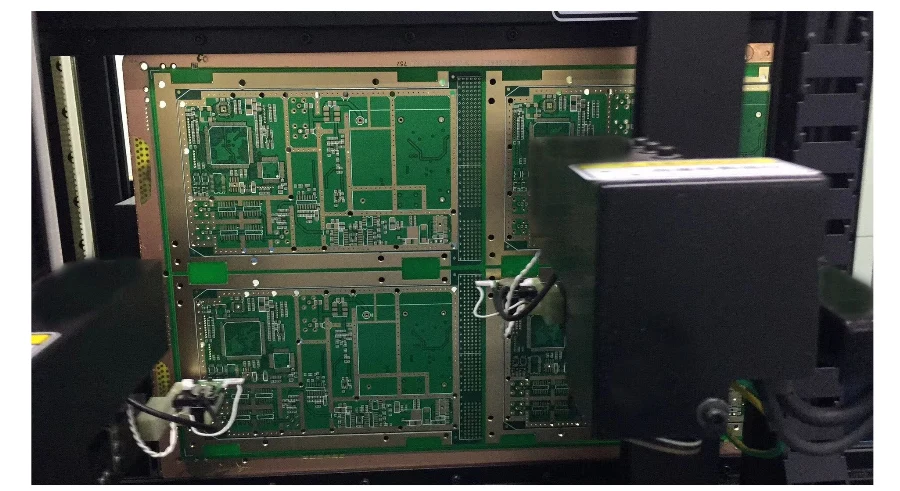
- A VCO PCB should be reviewed as a noise-sensitive RF control board, not as a generic clock or signal board.
- The first checks are resonator topology, tuning-line cleanliness, power filtering, ground continuity, output matching, and shielding around the active RF path.
- Most VCO problems show up as unstable tuning, poor phase-noise behavior, frequency drift, or measurement inconsistency rather than as total functional failure.
- Layout quality matters because the varactor control node, resonant network, bias circuits, and output path can all translate board noise into RF instability.
- Prototype validation should define the RF test path early, including cables, connectors, supply noise control, and the instruments used for frequency and phase-noise measurement.
A VCO PCB is the board that supports a voltage-controlled oscillator circuit and its bias, tuning, output, and filtering networks. It needs careful control of layout parasitics, supply cleanliness, grounding, shielding, and measurement setup because small electrical disturbances can directly affect tuning behavior, phase noise, output stability, and repeatability during RF test.
Contents
- What to review first on a VCO PCB
- Key design and verification rule table
- Early engineering risk table
- How layout and grounding affect phase noise and tuning stability
- How power filtering, shielding, and output matching should be reviewed
- What RF test and prototype teams should lock down before release
- FAQ
- Next steps
- References
- Author and review
What to review first on a VCO PCB
A VCO PCB is usually part of a larger synthesizer, signal-source, clocking, or RF front-end path. It is not just a frequency-generating block dropped onto a board. The oscillator core, tuning network, bias path, output buffer, and test interface all interact through parasitics, supply noise, and grounding. A circuit that looks correct in simulation can still perform poorly if the board adds noise or shifts the resonant behavior.The first review points are usually:
- which oscillator topology and tuning element the design uses and how sensitive the control node is to external noise
- whether the resonant path, active device, and output network are compact enough to avoid unnecessary parasitics
- whether the tuning voltage and supply rails are filtered, isolated, and easy to probe during bring-up
- whether the RF output path, launch, connector, and ground stitching preserve a predictable impedance environment
- how the board will actually be measured for frequency, output power, tuning linearity, phase noise, and drift
For higher-frequency or mixed RF builds, it is often useful to review stackup and material choices against high-frequency PCB and Rogers PCB constraints before layout freeze.
Key design and verification rule table
| Rule / parameter | What to check first | Why it matters | How to verify | If ignored | | --- | --- | --- | --- | --- | | Tuning-node cleanliness | Keep the control-voltage path short, filtered, and isolated from digital or switching noise | The tuning line can directly modulate oscillator behavior | Schematic review, layout review, powered noise measurement | Frequency instability, spurs, poor tuning repeatability | | Resonant-path compactness | Minimize unnecessary trace length and loop area around the oscillator core | Parasitics can shift frequency and degrade RF behavior | Placement review and RF layout inspection | Moved center frequency, lower margin, harder tuning | | Ground continuity | Maintain a clean RF return path with strong local stitching | Ground impedance affects phase noise, output quality, and shielding effectiveness | Layer review, via-stitch review, prototype measurement | Added noise, poor isolation, inconsistent results | | Power filtering | Isolate oscillator and buffer rails from wider board noise | Supply ripple and digital noise often appear as spurs or degraded phase noise | Filter review, supply-noise test, powered prototype check | Spur growth, degraded stability, measurement confusion | | Output matching and launch | Treat the output trace, launch, and connector as one RF path | Even short mismatches can distort the measured behavior | RF launch review, impedance check, [impedance calculator](/tools/impedance-calculator/) review | Return loss issues, output error, hard-to-compare data | | Test path definition | Lock down cable, connector, instrument, and fixture assumptions early | RF measurements are only useful when the setup is repeatable | Bring-up checklist, calibration plan, controlled prototype test | Inconsistent data and false design conclusions |Early engineering risk table
| Early signal | Typical root cause | Most affected area | Recommended action before pilot build | | --- | --- | --- | --- | | VCO tune line runs near digital control traces | Layout treated the tune node as a normal analog net | Frequency stability and spur performance | Re-route, filter, and isolate the control path before release | | Oscillator core is spread across a large area | Placement prioritized convenience over RF compactness | Start-up margin and repeatability | Tighten the resonant and bias loop placement | | Output connector is treated as purely mechanical | RF launch and ground transition were not reviewed | Measurement accuracy and output quality | Review connector footprint, launch geometry, and stitch vias | | Test setup is undefined until after assembly | Prototype goals were not linked to actual RF measurement flow | Validation and debug speed | Freeze cables, fixtures, calibration assumptions, and test sequence early |How layout and grounding affect phase noise and tuning stability
Most VCO PCB problems start where sensitive RF behavior meets ordinary board noise. The tuning port, active device bias, resonant network, and output stage all respond to parasitic capacitance, return-path discontinuities, and nearby switching activity. The board should therefore be organized around electrical sensitivity, not just around component grouping.Three layout decisions usually dominate the result.
1. Keep the resonant structure physically tight
The oscillator core should avoid long traces, unnecessary vias, and broad loop geometry. Extra inductance and capacitance can shift the usable tuning range or change how the design behaves across process and temperature variation. If the design is running well into RF territory, high-frequency PCB construction may be a better fit than treating it like a generic FR-4 control board.
2. Protect the tuning node from low-frequency and switching noise
The tuning line often looks electrically slow, but it is one of the most sensitive nets on the board. Noise on this path can become frequency modulation or create visible sidebands in measurement. Filter placement, shielding distance, and routing separation matter more than simply adding another capacitor at random.
3. Make the ground strategy local and intentional
Ground stitching around the oscillator region, output launch, and shielding boundaries should support the actual RF return path. Large ground areas are useful only when they are connected in ways that preserve continuity. A review in Gerber viewer is often the fastest way to catch fractured returns, poor via fences, or awkward launch geometry before fabrication.
How power filtering, shielding, and output matching should be reviewed
VCO performance depends on more than the oscillator core. Power delivery, shielding approach, and output termination all affect whether the measured result is stable and believable.The most common review points are:
- whether the oscillator rail is separated from switching regulators, digital control, or noisy shared analog rails
- whether the board needs local shielding cans, grounded enclosure features, or denser via fencing around the RF region
- whether the output buffer and launch were designed for the measurement environment the lab will actually use
- whether temperature rise, airflow assumptions, or nearby hot components can move the oscillator behavior during test
If the design needs cleaner RF behavior, better launch control, or tighter material consistency, teams often need to align Rogers PCB, high-frequency PCB, and PCB prototype planning before ordering the first spin.
What RF test and prototype teams should lock down before release
A VCO PCB can easily create misleading test results if the measurement path is undefined. Before prototype release, the board team and test team should agree on what the first build is supposed to prove and how that proof will be measured.A practical validation plan usually includes:
- Prototype objective defined early
Decide whether the first build is for start-up confirmation, tuning characterization, phase-noise evaluation, temperature behavior, or production-oriented manufacturability. - Controlled RF output path
Freeze the connector type, cable assumptions, terminations, and instrument connection path before measurements begin. - Power and tuning measurement access
Provide safe, repeatable probing points for supply rails, tune voltage, enable logic, and any lock-detect or monitor outputs. - Assembly and inspection route
Confirm whether the package mix, shield cans, and connector density require AOI, X-ray, or tighter first-article review. SMT assembly planning matters if the RF section uses fine-pitch or thermally sensitive parts. - Build-data and BOM control
Record revision state, substitutions, and setup assumptions so measured behavior can be compared across spins. A BOM viewer review helps catch mismatched alternates before assembly.
If the project is moving quickly from lab validation into coordinated sourcing and build, turnkey assembly and quick-turn PCB support usually reduce debug noise caused by fragmented handoffs.
FAQ
What is the first thing to check when a VCO PCB has unstable frequency output?
Start with the tune-voltage path, power cleanliness, grounding, and the physical compactness of the oscillator core. Many instability problems come from board-level noise or parasitics rather than from the active device alone.
Does a working oscillation mean the VCO PCB is designed correctly?
No. A VCO can oscillate and still have poor phase noise, spur performance, tuning linearity, or temperature stability. Functional start-up is only the first check.
When should a VCO board use RF materials instead of standard FR-4?
That depends on operating frequency, loss budget, launch sensitivity, and repeatability needs. Higher-frequency designs or tighter RF margins often justify a review against Rogers PCB or other RF-focused constructions.
Why is the tuning line so critical on a VCO PCB?
Because the tuning line directly influences oscillation frequency. Noise or coupling on that path can show up immediately as modulation, sidebands, drift, or poor tuning repeatability.
What should be frozen before the first VCO prototype release?
Freeze the oscillator topology assumptions, tune-line filtering approach, stackup, RF launch path, probing plan, and the exact measurement setup for the first validation round.
Next steps
If you are developing a VCO PCB, the most useful next step is usually to review the oscillator region, tune path, output launch, and RF test setup together instead of treating them as separate tasks.HILPCB can support that process through:
- High-frequency PCB planning when the oscillator path needs cleaner RF behavior
- Rogers PCB review when material stability and RF loss become important design constraints
- SMT assembly alignment for fine-pitch, shielded, or RF-sensitive assemblies
- Turnkey assembly support when fabrication, assembly, and RF test preparation need to stay coordinated
- PCB prototype and quick-turn PCB support for first-spin validation
- Request a quote when your layout package, BOM, and test notes are ready for review