
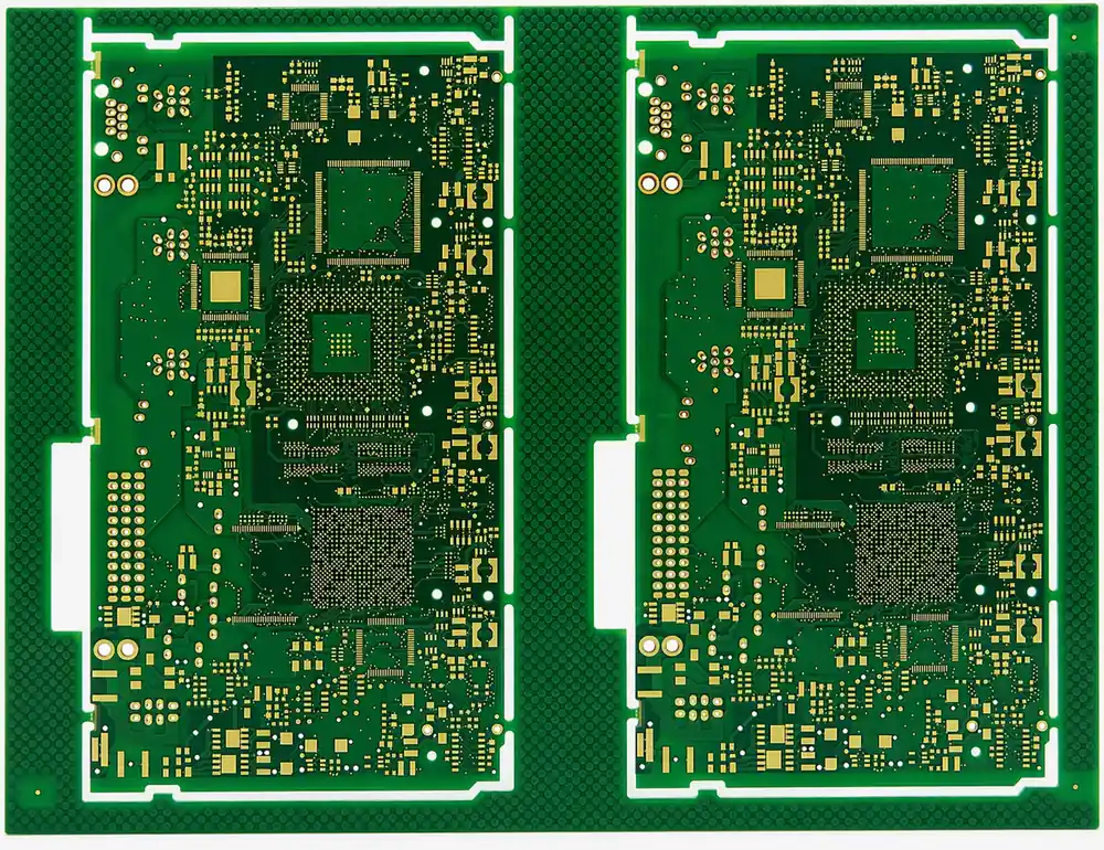
16 layer PCBs represent the layer count where power delivery network (PDN) design becomes as critical as signal integrity. Boards at this complexity routinely serve high-performance processors, FPGAs, and SoCs that draw 50-200A of total current across 8-12 different voltage rails. Supplying stable, low-noise power to these devices—while simultaneously routing hundreds of high-speed signals—demands a stack-up architecture where power plane allocation, copper weight selection, and decoupling strategies are engineered with the same rigor as impedance control.
Before copper weights and plane allocation harden, it is usually worth reviewing heavy copper PCB process constraints together with high Tg PCB material stability for power-dense builds.
But a 16 layer PCB is not only about power. Designs at this layer count span everything from FPGA-based signal processing boards and EV motor controllers to telecom base station digital units and high-reliability industrial control systems. Some use standard 1oz copper throughout; others integrate heavy copper (2-4oz) on power plane layers for high-current distribution. Some are pure FR-4; others combine low-loss dielectrics on high-speed signal layers with standard FR-4 elsewhere.
This guide examines 16 layer PCB manufacturing through the lens of power integrity—because this is the engineering challenge that distinguishes 16 layer designs from lower layer counts—while also covering the material, via, and process options relevant across all 16 layer applications. In practice, many teams end up reviewing these decisions against wider multilayer PCB stack-up constraints before release.
Power electronics engineers across Germany, Texas, and Ontario rely on HILPCB's heavy copper processing expertise for EV inverter boards and industrial motor drive platforms where current capacity is mission-critical.
HILPCB Manufacturing Capability: We fabricate 16 layer PCBs with mixed copper weights from 0.5oz to 4oz on inner layers, controlled impedance to ±8%, and power integrity-optimized stack-ups supporting designs with 10+ voltage domains—from quick-turn prototype through volume production.
In This Guide
- Why 16 Layers: The Power Distribution Inflection Point
- Stack-Up Architecture for Power Integrity
- Multi-Voltage Plane Design and Copper Island Partitioning
- Heavy Copper Inner Layers: Process and Design Rules
- Decoupling Strategy and PDN Via Design
- Thermal Management Through Board Structure
- Lamination Engineering for Mixed Copper Weights
- Material Selection for 16 Layer Boards
- 16 Layer HDI, Rigid-Flex, and Specialty Constructions
- Engineering Support for Power-Critical Designs at HILPCB
Why 16 Layers: The Power Distribution Inflection Point
Modern high-performance ICs create demanding power delivery requirements. A large FPGA (Xilinx UltraScale+ or Intel Agilex class) may require separate voltage rails for: core logic (0.72-0.85V at 30-60A), I/O banks (1.2V, 1.8V, 2.5V, 3.3V each at 5-15A), auxiliary power (1.8V at 2-5A), transceivers (0.9V at 10-20A), and configuration (3.3V at 1-2A). That is 8-10 independent voltage domains for a single IC.When the design includes an FPGA plus DDR memory, a network processor, Ethernet PHYs, and peripheral interfaces, the total voltage rail count exceeds 12 and total current can reach 200A. At 12 layers, the designer has only 2-3 power plane layers—forcing extensive plane splitting that degrades PDN impedance. At 16 layers, 5-6 dedicated power plane layers become available, enabling each high-current rail to have its own unbroken plane or generous copper island.
Stack-Up Architecture for Power Integrity
The optimal 16 layer stack-up for power-intensive designs prioritizes tightly coupled ground-power plane pairs for distributed decoupling, heavy copper planes for low DC resistance, and sufficient signal layers for all high-speed interfaces.Power-Optimized 16 Layer Stack-Up
| Layer | Function | Copper Weight | Notes |
|---|---|---|---|
| L1 | Signal (Top) | 1oz | Component side |
| L2 | Ground Plane | 1oz | Unbroken reference |
| L3 | Signal | 0.5oz | High-speed routing |
| L4 | Power Plane (VDD Core) | 2oz | High-current FPGA core |
| L5 | Ground Plane | 2oz | PDN pair with L4 |
| L6 | Signal | 0.5oz | High-speed routing |
| L7 | Power Plane (VDD I/O) | 1oz | I/O voltage rails |
| L8 | Ground Plane | 1oz | Central reference |
| L9 | Ground Plane | 1oz | Central reference |
| L10 | Power Plane (VDD Trans) | 1oz | Transceiver power |
| L11 | Signal | 0.5oz | General routing |
| L12 | Ground Plane | 2oz | PDN pair with L13 |
| L13 | Power Plane (Secondary) | 2oz | 3.3V, 5V rails |
| L14 | Signal | 0.5oz | General routing |
| L15 | Ground Plane | 1oz | Unbroken reference |
| L16 | Signal (Bottom) | 1oz | Component side |
The key PDN features are the tightly coupled power-ground pairs (L4-L5 and L12-L13). When separated by thin dielectric (2-3mil), they form a parallel plate capacitor with significant distributed capacitance—typically 200-400pF/cm²—providing high-frequency decoupling that discrete capacitors cannot match above 500MHz.
The L8-L9 double ground plane pair at the center creates an electromagnetic barrier between upper and lower halves, provides a low-impedance return path for via transitions, and adds mechanical symmetry critical for warpage control in thick 16 layer boards.
Multi-Voltage Plane Design and Copper Island Partitioning
With 8-12 voltage rails and only 4-6 power plane layers, each power plane must carry multiple voltage domains through copper island (split plane) design.Plane Partitioning Rules
- Minimum island width: 50mil (1.27mm) for adequate current capacity and reliable etching
- Clearance between islands: 20mil (0.5mm) minimum standard, 15mil advanced
- Isolation testing: Fabricator must verify islands are properly isolated—no copper debris or plating artifacts bridging the gap
Voltage Rail Allocation Strategy
Assign voltage rails based on current demand: highest-current rails (>20A) get a full plane on a 2oz or 3oz copper layer. The FPGA core voltage, drawing 30-60A, should have its own dedicated plane. Medium-current rails (5-20A) share a plane as separate islands—ensure the copper area supports the current density (target <15A/mm² for 1oz, <30A/mm² for 2oz). Low-current rails (<5A) can be routed as wide power traces (20-50mil) on signal layers, freeing plane layers for higher-current domains.
The Critical Rule: No Signals Over Plane Splits
Never route signals on a layer directly above or below a split plane boundary. The split breaks the return current path, creating a slot antenna that radiates noise and destroys signal integrity. In a 16 layer stack-up, designate signal layers adjacent to split power planes for signals that only run within a single voltage domain's copper island area.
 Microsection of a 16 layer PCB showing 2oz heavy copper power planes with complete prepreg resin fill between copper features. Proper resin fill prevents dielectric voids that would compromise voltage isolation and long-term reliability under thermal cycling—a critical manufacturing control for power-dense designs serving automotive EV, industrial motor drive, and telecommunications applications.
Heavy Copper Inner Layers: Process and Design Rules
Integrating 2oz-3oz copper on inner layers of a 16 layer board requires modified fabrication processes compared to standard 1oz construction.Etching Impact on Feature Size
Heavy copper requires longer etch times, causing greater lateral etch (undercut). Design rules must specify different minimum features per copper weight:
| Copper Weight | Thickness | Min Trace Width | Min Space | Lateral Etch |
|---|---|---|---|---|
| 0.5oz | 17.5μm | 3mil | 3mil | ~12μm/side |
| 1oz | 35μm | 3.5mil | 3.5mil | ~15μm/side |
| 2oz | 70μm | 5mil | 5mil | ~25μm/side |
| 3oz | 105μm | 6mil | 6mil | ~35μm/side |
| 4oz | 140μm | 8mil | 8mil | ~45μm/side |
Prepreg Resin Fill Requirements
Heavy copper patterns create deep etch profiles that must be completely filled by prepreg resin during lamination. A 2oz layer has 70μm deep trenches—requiring substantially more resin than 1oz. The fabricator selects high-resin-content prepreg (e.g., 7628 glass style with 50-60% resin content). Insufficient fill causes air pockets (voids) that reduce voltage withstand capability and lead to delamination during thermal cycling.
Decoupling Strategy and PDN Via Design
Effective PDN design at 16 layers combines embedded plane capacitance with strategically placed discrete decoupling capacitors, all connected through low-inductance via structures.Frequency-Based Decoupling
- Bulk (100-470μF, electrolytic/tantalum): Within 25mm of high-current ICs, targeting 10kHz-1MHz. Connect with 4-8 vias per pad.
- Mid-frequency (1-10μF MLCC, 0402/0603): Within 10mm, targeting 1-100MHz. Minimum 2 vias per pad.
- High-frequency (10-100nF MLCC, 0201/0402): Directly beneath BGA packages (underside of board), targeting 100MHz-1GHz. Via design is critical—the total loop inductance must be minimized.
Low-Inductance PDN Via Design
A single through-hole via has approximately 0.5-1nH of inductance—at 500MHz, this represents 1.5-3Ω impedance, far exceeding milliohm PDN targets. Solutions: use 4-6 parallel vias per power/ground connection (N parallel vias have inductance L/N), place power and ground vias as close as possible (adjacent pads) to minimize loop area, and use blind vias from the component layer directly to the target power plane to eliminate unused stub inductance.
Thermal Via Arrays
For ICs with exposed thermal pads, thermal via arrays (0.3mm diameter, 1.0-1.2mm pitch, filled with non-conductive epoxy and capped) transfer heat from the component pad to inner copper planes. With 2oz inner planes, thermal dissipation capacity is doubled versus 1oz. For extreme loads (>10W per component), embedded copper coins or metal core integration provides a direct thermal path.
Thermal Management Through Board Structure
16 layer boards with heavy copper and high power density generate significant heat within the board structure. Each copper plane acts as a lateral heat spreader—copper's thermal conductivity (385 W/mK) is ~1000× higher than FR-4 dielectric (0.3 W/mK). With 2oz copper planes, thermal spreading is doubled compared to 1oz.For the most demanding thermal applications, a 16 layer construction can incorporate an aluminum or copper metal core as the center substrate, with rigid layers built up on both sides using thermally conductive dielectric. The metal core is electrically isolated but provides board-level heat spreading far exceeding what copper planes alone achieve.
Lamination Engineering for Mixed Copper Weights
Mixed copper weights require modified press parameters:- Temperature ramp: 1.5-2.0°C/min (vs. standard 2.5-3.0°C/min) to allow resin flow before gelation
- Initial pressure: 350-500 PSI (vs. standard 300-400 PSI) to drive resin into deep channels
- Cure time: 120-150 minutes (vs. standard 90 minutes) for complete cross-linking
Mixed weights must be distributed symmetrically about the stack-up center—if L4 is 2oz, L13 should also be 2oz. Asymmetric distribution causes differential stress during cooling, resulting in board warpage.
Material Selection for 16 Layer Boards
### FR-4 GradesHigh-Tg FR-4 (Tg ≥170°C) is mandatory for 16 layer boards—the longer lamination cycles and multiple reflow temperatures during assembly create thermal stress that standard FR-4 cannot reliably withstand. ITEQ IT-180A, Isola 370HR, and Shengyi S1000-2 are standard choices.
Hybrid Material Stack-Ups
For 16 layer designs with high-speed serial interfaces (PCIe Gen 4/5, 25GbE), signal layers carrying these channels benefit from low-loss dielectrics (Megtron 4/6, I-Speed) while power and ground planes remain on standard FR-4. This approach reduces material cost by 30-40% versus an all-low-loss construction.
Halogen-Free and Automotive-Grade
For automotive applications (IATF 16949), halogen-free high-Tg materials are increasingly specified. These process with 5-10% higher lamination pressure and modified drill parameters.
Impedance Control on 16 Layer Power-Dense Boards
Signal integrity on 16 layer boards with heavy copper presents a unique challenge: the thick copper on power planes affects the dielectric thickness available for adjacent signal layers, directly changing impedance. If a signal layer is separated from a 2oz power plane by 4mil prepreg, the actual pressed dielectric may be only 3-3.5mil because the 70μm copper relief is partially filled by resin from the prepreg.
Compensating for Heavy Copper Effects
The impedance simulation must use the actual post-press dielectric thickness—not the nominal prepreg thickness. HILPCB's DFM review accounts for this by modeling the resin fill around heavy copper features and calculating the effective dielectric thickness for each layer pair. Without this compensation, impedance can be 5-10% lower than expected on layers adjacent to heavy copper planes.
Common Impedance Targets at 16 Layers
| Interface | Target | Layer Assignment |
|---|---|---|
| DDR4/DDR5 DQ | 40Ω SE / 80Ω diff | L3 or L14 |
| PCIe Gen 4/5 | 85Ω differential | L6 or L11 |
| USB 3.x / USB4 | 90Ω differential | L6 or L11 |
| Gigabit Ethernet | 100Ω differential | L14 |
| LVDS / HDMI | 100Ω differential | Any stripline |
| General I/O | 50Ω SE | L1 or L16 |
DFM Rules Specific to 16 Layer Power-Dense Designs
Power Plane Design Rules
- IR drop calculation: For high-current planes (>20A), verify that the copper area and thickness provide <5% voltage drop from VRM output to the farthest IC power pin. Use plane-to-plane current density ≤30A/mm² for 2oz copper.
- Split plane clearance: Maintain ≥20mil clearance between voltage islands with different potentials. Add guard traces (ground connections) between high-voltage islands (≥12V) and low-voltage domains.
- Via thermal relief: Power plane connections to through-hole vias must use thermal relief pads (4 spokes, 10mil spoke width) to ensure solder wetting during assembly. Direct connections on power planes make hand-soldering and rework extremely difficult.
Signal Routing Rules for Heavy Copper Boards
- Route high-speed signals adjacent to 1oz planes, not 2oz: The higher profile of 2oz copper creates impedance uncertainty due to etch profile variation. Assign high-speed layers adjacent to standard-weight ground planes.
- Back-drilling on power-dense boards: When power vias (large hole, 0.4-0.5mm) and signal vias (0.2-0.3mm) share the same area, back-drill only signal vias—power vias do not create resonance problems at the frequencies of concern.
- Decoupling via placement: Place decoupling capacitor vias as close to IC power pins as the BGA pitch allows. For 0.8mm pitch BGAs, use blind microvias for decoupling to avoid through-via congestion beneath the device.
Testing and Verification for 16 Layer Boards
Electrical Testing
100% continuity and isolation testing is mandatory. For 16 layer boards with mixed copper, electrical test fixtures must accommodate the thicker board (typically 2.0-2.8mm).
Impedance Verification
TDR coupon measurement on 6-8 impedance structures per panel verifies each unique layer combination. For power-dense designs, additional through-via impedance measurements confirm that PDN via inductance is within specification.
Thermal Reliability
IST (Interconnect Stress Test) coupons verify that through-hole vias spanning the full 16 layer stack (2.0-2.8mm, aspect ratio 7-10:1) with mixed copper weights survive 200+ thermal cycles. Heavy copper via barrels experience higher CTE-induced stress than standard copper—IST confirms long-term reliability.
16 Layer HDI, Rigid-Flex, and Specialty Constructions
### HDI at 16 Layers16 layer designs with dense BGA packages at 0.5mm pitch often require blind vias for signal escape. A 1+14+1 structure adds laser-drilled microvias from L1-L2 and L15-L16, freeing inner routing channels beneath component footprints.
Rigid-Flex at 16 Layers
16 layer rigid-flex boards serve applications in military avionics, medical imaging systems, and complex industrial controllers where multiple rigid PCB sections must interconnect without connectors. A typical 16R-4F configuration runs 4 flex layers through the flex zone with 12 additional rigid layers in rigid sections.
Engineering Support for Power-Critical Designs at HILPCB
Power integrity failures on 16 layer boards are expensive to diagnose and even more expensive to fix in production. HILPCB's DFM review for power-dense designs includes stack-up impedance analysis, copper weight recommendations, and prepreg resin fill calculations—identifying potential issues before they reach the lamination press.Heavy Copper Processing: Inner layers from 0.5oz to 4oz with mixed copper weights. Differential etching compensation for feature size accuracy.
PDN-Optimized Stack-Ups: DFM review includes PDN impedance analysis. Tight dielectric coupling (2-3mil prepreg) for embedded plane capacitance.
Thermal Solutions: Thermal via arrays, copper coin embedding.
Impedance Control: ±8% on signal layers, TDR-verified. Comprehensive coupon sets for each unique impedance geometry.
Material Options: Standard FR-4, high-Tg, mid-loss, low-loss, halogen-free, and thermally conductive dielectrics.
Quality: IPC-A-600 Class 3, IST (Interconnect Stress Testing) for heavy copper via integrity, 100% electrical testing with full SPC.
Production: 7-day express prototypes through volume production with full lot traceability. Turnkey SMT assembly available.
Submit your 16 layer power-dense design for a free PDN stack-up review →