
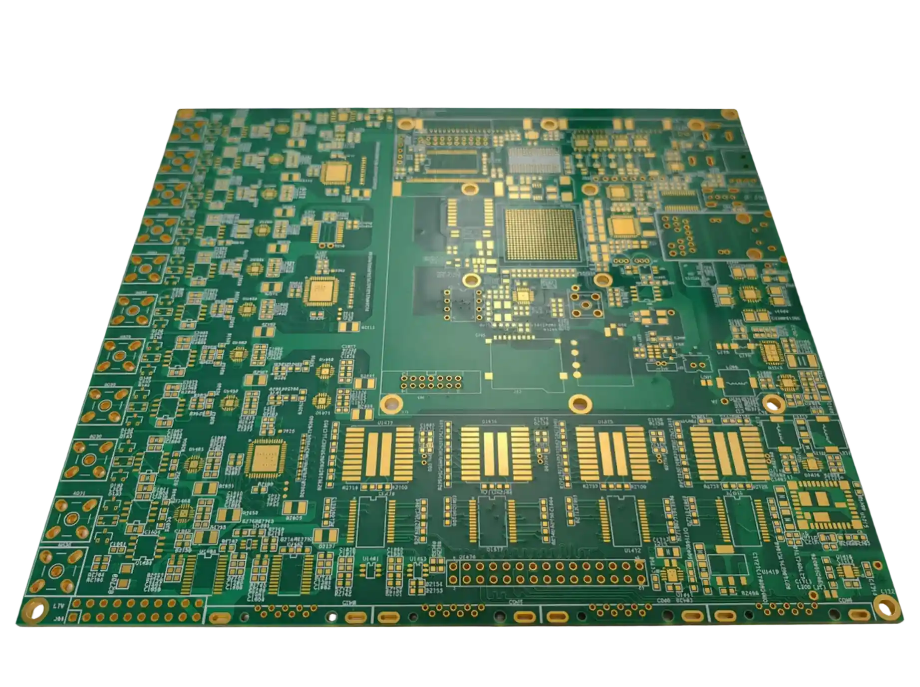
18 layer PCBs are the go-to architecture for systems that must combine high-frequency RF circuits with complex digital baseband processing on a single board. At this layer count, the design has enough layer budget to accommodate dedicated RF signal layers using low-loss dielectric materials (Rogers, PTFE, Megtron) alongside digital routing layers on standard FR-4—each material system placed precisely where its electrical properties are needed, without the compromises that lower layer counts force.
The manufacturing challenge that distinguishes 18 layer hybrid PCBs from standard multilayer boards is multi-material lamination: bonding dissimilar dielectrics with different thermal expansion rates, maintaining impedance accuracy across materials with different Dk values, and managing the registration complexity of 18 individual layers through multiple lamination cycles. This is not standard PCB manufacturing—it is precision materials engineering.
This guide covers the complete fabrication process for 18 layer PCBs with emphasis on hybrid material constructions, the processing differences between Rogers, PTFE, and Megtron material families, impedance engineering across material boundaries, and the via transition designs that preserve signal quality when signals cross from one dielectric environment to another.
RF design teams across the Nordic telecom sector, UK defense contractors, and North American 5G infrastructure companies partner with HILPCB for hybrid material stack-ups that demand both RF performance and digital density—because our lamination expertise, material inventory, and VNA verification capability are what turn a designer's hybrid stack-up concept into a reliable, production-grade PCB.
HILPCB Manufacturing Capability: We manufacture 18 layer hybrid PCBs combining Rogers 4350B/4003C, PTFE/Teflon, Megtron 6/7, and FR-4 in engineered stack-ups with impedance control to ±5% on RF layers and ±8% on digital layers, verified by TDR and VNA measurement to 20GHz.
In This Guide
- When 18 Layers Are Needed for RF/Digital Integration
- The Material Families: Rogers, PTFE, Megtron, and FR-4
- Hybrid Stack-Up Design: Placing Materials Where They Matter
- Impedance Engineering Across Mixed Dielectrics
- Multi-Material Lamination Process
- Via Transitions Between RF and Digital Domains
- Full Low-Loss 18 Layer Constructions
- Manufacturing Tolerances and Quality Verification
- Partnering with HILPCB for 18 Layer Hybrid Fabrication
When 18 Layers Are Needed for RF/Digital Integration
Modern wireless and radar systems increasingly integrate RF front-end circuits with digital signal processing on a single board. This eliminates inter-board RF connections—every connector, cable, and board-to-board transition introduces insertion loss, impedance mismatch, and a potential failure point. Typical 18 layer RF/digital hybrid designs include:- 5G base station radio units combining mmWave or sub-6GHz front-end with digital beamforming FPGA
- Phased array radar modules with integrated T/R modules and signal processing
- Satellite communication transponders with frequency conversion and digital modulation/demodulation
- Electronic warfare systems with wideband receivers and real-time digital signal processing
- Automotive radar modules (24GHz and 77GHz) combining RF front-end with MCU-based processing
These systems demand RF routing layers with dielectric loss factors (Df) below 0.004 at 10GHz—a performance level that standard FR-4 (Df 0.020) cannot remotely achieve. Simultaneously, the digital section requires 8-10 routing layers for high-pin-count FPGAs, DDR memory interfaces, and high-speed serial links.
An 18 layer stack-up can allocate 4-6 layers on RF-grade materials for antenna, filter, and transceiver circuits, while the remaining 12-14 layers use FR-4 or mid-loss material for digital routing and power distribution.
The Material Families: Rogers, PTFE, Megtron, and FR-4
Each high-frequency material family has distinct electrical properties, processing characteristics, and cost implications.Rogers 4000 Series
Rogers 4003C (Dk 3.38, Df 0.0027 at 10GHz) and 4350B (Dk 3.48, Df 0.0037 at 10GHz) are thermoset hydrocarbon laminates reinforced with woven glass and engineered fillers. They are the most practical choice for hybrid stack-ups because their CTE (11-14 ppm/°C X-Y) is close to FR-4 (14-17 ppm/°C), they process with standard drill bits and etching chemistry, and standard FR-4 prepreg or Rogers 4450F bondply can bond Rogers to FR-4.
Processing differences from FR-4: 20% reduced drill feed rates (Rogers is slightly softer), modified desmear chemistry (reduced permanganate process time), and careful solder mask adhesion (surface preparation may need adjustment). These are well-understood modifications that any experienced high-frequency fabricator handles routinely.
PTFE-Based Materials
PTFE (Polytetrafluoroethylene) laminates—including Rogers RT/duroid 5880 (Dk 2.20, Df 0.0009) and Taconic TLY (Dk 2.20, Df 0.0009)—provide the lowest dielectric loss available, essential for mmWave frequencies up to 77GHz. However, PTFE is significantly harder to process:
- Drilling: PTFE is extremely soft and waxy, causing drill loading. Special drill geometries with higher helix angles and reduced chip load are required. Laser drilling produces superior results.
- Copper adhesion: Inherently poor (2-4 lb/in peel strength). Sodium etchant surface treatment or plasma roughening is mandatory (target ≥6 lb/in).
- CTE mismatch: PTFE's high CTE (24 ppm/°C X-Y) versus FR-4 (14-17 ppm/°C) limits PTFE to 2-4 layers within an 18 layer hybrid stack—more PTFE layers increase delamination risk at material boundaries.
Panasonic Megtron Series
Megtron 6 (Dk 3.4, Df 0.002 at 10GHz) and Megtron 7 (Dk 3.3, Df 0.001) offer a middle ground: significantly better loss performance than FR-4, with processing characteristics closer to FR-4 than PTFE. They are glass-reinforced, providing better dimensional stability than PTFE, and can be drilled with standard equipment. Megtron is increasingly popular for 18 layer designs where all signal layers need low-loss performance—100G+ networking equipment, for example.
Material Selection Decision Framework
| Frequency Range | Recommended Material | Df (10GHz) | Processing Difficulty |
|---|---|---|---|
| ≤1 GHz | Standard FR-4 | 0.020 | Standard |
| 1-6 GHz | Rogers 4350B or Megtron 4 | 0.004-0.005 | Moderate |
| 6-20 GHz | Megtron 6 or Rogers 4003C | 0.002-0.003 | Moderate |
| 20-40 GHz | Megtron 7 or Rogers RO3003 | 0.001-0.002 | Moderate-High |
| 40-77 GHz | PTFE (RT/duroid 5880) | 0.0009 | High |
Hybrid Stack-Up Design: Placing Materials Where They Matter
### RF Top + Digital Bottom ConfigurationThe most common hybrid approach places RF-grade material on the top layers and FR-4 on the remaining layers:
| Layer | Function | Material | Dk | Df (10GHz) |
|---|---|---|---|---|
| L1 | RF Signal (Top) | Rogers 4350B | 3.48 | 0.0037 |
| L2 | Ground Plane | Copper | — | — |
| L3 | RF Signal | Rogers 4350B | 3.48 | 0.0037 |
| L4 | Ground Plane | Bondply interface | — | — |
| L5-L18 | Digital signal/power/ground | FR-4 High-Tg | 4.3 | 0.020 |
This works well for designs where the RF section is physically located on one side of the board (antenna elements, filters, LNA on top) and the digital section on the other.
Symmetric Hybrid Configuration
For dual-band systems or phased arrays with RF elements on both board faces:
- L1-L3: Rogers 4350B (RF front-end A)
- L4-L15: High-Tg FR-4 (Digital core)
- L16-L18: Rogers 4350B (RF front-end B)
Symmetry simplifies lamination because thermal expansion forces balance, significantly reducing warpage.
Full Megtron 18 Layer Stack-Up
When both RF and digital signals require low-loss performance—such as in 100G+ networking switches or high-performance radar signal processors—the entire 18 layer stack can use Megtron 6 or Megtron 7. All signal layers benefit from Df ≤0.002, eliminating material boundaries and the impedance discontinuities they create. Cost is 3-6× standard FR-4, but the material consistency simplifies stack-up design and eliminates CTE mismatch concerns.
Impedance Engineering Across Mixed Dielectrics
### Dk Impact on Trace WidthThe same impedance target requires different trace widths on different materials. For 50Ω microstrip with 4mil dielectric, 1oz copper:
| Material | Dk | Trace Width for 50Ω |
|---|---|---|
| FR-4 | 4.3 | 7.0mil |
| Rogers 4350B | 3.48 | 8.2mil |
| Megtron 6 | 3.4 | 8.5mil |
| PTFE RT/5880 | 2.20 | 11.5mil |
Via transitions carrying 50Ω signals from FR-4 to Rogers layers require a trace width change at the layer transition—the layout tool must be configured with different impedance rules per layer.
Dk Tolerance and Achievable Impedance
Rogers 4350B specifies Dk = 3.48 ± 0.05 (±1.4%), while standard FR-4 specifies Dk = 4.3 ± 0.3 (±7%). This tighter Rogers Dk tolerance enables ±5% impedance tolerance on RF layers versus ±8-10% on FR-4—a meaningful difference for RF filter and matching circuit performance.
Frequency-Dependent Dk Variation
Both materials exhibit Dk change with frequency, but the magnitude differs dramatically: FR-4's Dk drops approximately 10% from 100MHz to 10GHz, while Rogers 4350B varies less than 1%. For broadband RF circuits operating across a wide frequency range, Rogers' Dk stability provides more consistent impedance performance.
Simulation and Modeling for Hybrid Stacks
HILPCB performs 2D field solver simulation using actual material Dk/Df parameters for each layer during DFM review. For hybrid designs, the simulation uses the bondply Dk at material interfaces, not the adjacent laminate Dk—an error that can cause 5-8% impedance deviation if overlooked. For critical RF designs, we provide S-parameter simulation of via transitions using 3D full-wave solvers.
 Cross-section of an 18 layer hybrid PCB showing Rogers 4350B RF layers (top) bonded to a high-Tg FR-4 digital core using Rogers 4450F bondply. This mixed-material construction enables both low-loss RF performance above 10GHz and high-density digital routing on a single board—the manufacturing approach used for 5G radio units, phased array radar modules, and satellite communication transponders produced at HILPCB for telecom and defense customers across Europe and North America.
DFM Rules for 18 Layer Hybrid Boards
Material Interface Rules
- Copper relief at material boundaries: Avoid large unbroken copper areas (>20mm×20mm) at the Rogers-FR-4 interface—CTE mismatch concentrates stress at the edges of large copper features.
- Via placement at boundaries: Specify copper-filled vias at material transitions where signals cross from one material to another. Filled vias distribute stress better than hollow vias.
- Bondply thickness minimum: ≥3mil to ensure adequate resin flow and bond strength. Thinner bondply risks starved bonds at the interface.
RF Layer Routing Rules
- 50Ω ground-backed coplanar waveguide (GCPW): Preferred over simple microstrip for RF traces on outer layers. The coplanar ground conductors provide additional shielding and improve impedance control.
- RF trace length matching: For phased array and beamforming applications, RF trace length matching to within ±0.5° of electrical length at the operating frequency.
- Component exclusion zones: Keep digital components and their associated switching noise at least 5mm from RF routing on the same surface layer.
18 Layer Rigid-Flex Option
For defense and aerospace applications requiring connector-free board-to-board connections, 18 layer rigid-flex boards carry 2-4 flex layers through the flex zone. In hybrid material designs, the flex layers typically use polyimide (not Rogers or PTFE, which cannot bend), limiting flex connectivity to digital signals.
Cost Optimization for 18 Layer Hybrid Boards
| Design Choice | Cost Impact | Performance Impact |
|---|---|---|
| Rogers on all 18 layers | +300-500% material | Best RF performance on all layers |
| Rogers on RF layers + FR-4 elsewhere | +50-100% material | Optimized per layer |
| Megtron 6 on all layers | +200-300% material | Good RF + excellent digital |
| FR-4 only (no hybrid) | Baseline | RF performance limited |
The most cost-effective approach: use Rogers or Megtron only on the specific layers that require low-loss performance, and standard high-Tg FR-4 on all other layers. This typically adds 50-100% to material cost versus all-FR-4—a fraction of the cost of a full Rogers build—while delivering the RF performance needed.
Multi-Material Lamination Process
### Bondply and Prepreg SelectionThe bonding layer between dissimilar materials must adhere to both surfaces while maintaining acceptable dielectric properties:
- Rogers 4450F bondply (Dk 3.54, Df 0.004): Designed specifically for bonding Rogers 4000 series to FR-4. Cures at standard FR-4 temperatures.
- Standard FR-4 prepreg: Can bond Rogers 4350B/4003C to FR-4. Lowest cost but slightly less consistent Dk at the interface.
- PTFE bondply (Rogers 3001): Required for bonding PTFE materials—standard prepreg does not adhere to PTFE surfaces.
Sequential Lamination for Hybrid Stacks
18 layer hybrid boards typically require 2-3 lamination cycles: fabricate the FR-4 inner core (e.g., L5-L14) as a standard multilayer board, then laminate Rogers layers (L1-L4 and L15-L18) using bondply in a second press cycle. Each cycle subjects previously laminated layers to additional thermal stress, requiring high-Tg core material (Tg ≥170°C).
CTE Management at Material Boundaries
The X-Y CTE mismatch between Rogers (11-14 ppm/°C) and FR-4 (14-17 ppm/°C) creates shear stress at the boundary during temperature excursions. For a 200mm × 300mm board with 100°C temperature rise, differential expansion is approximately 30-60μm—enough to crack plated through-hole vias if not managed.
Mitigations: use Rogers 4000 series (lowest CTE mismatch), avoid large unbroken copper at boundaries (which concentrates stress), and specify filled vias at material transition regions.
Via Transitions Between RF and Digital Domains
Signal vias crossing between RF layers and digital layers are critical points for impedance matching and EMI containment.RF Via Design Rules
- Ground via fencing: Every signal via transitioning between domains must be surrounded by 4-8 ground vias within one via diameter distance. These provide complete return current paths and suppress cavity resonances.
- Anti-pad optimization: Anti-pad diameter directly affects via impedance—typically 30-40mil for a 10mil hole at 50Ω. Simulation is required for precise tuning.
- Back-drilling: Via stubs from signal entry points must be removed. For signals entering at L3 and routing to L7, both the L1-L3 stub above and the L7-L18 stub below should be back-drilled for channels above 10GHz.
Full Low-Loss 18 Layer Constructions
For designs where all signal layers carry high-speed data—such as [100G+ networking switches](/products/backplane-pcb/) or high-performance computing platforms—the entire 18 layer stack-up may use Megtron 6 or Megtron 7. This eliminates Dk discontinuities at layer transitions but increases material cost by 3-6×.The laminate supplier provides matched core and prepreg products (e.g., Megtron 6 core R-5775K with Megtron 6 prepreg R-5670K) with consistent Dk ± 0.05 across all thicknesses. Using a single material system simplifies impedance simulation and eliminates the via impedance discontinuities that hybrid stacks create.
Full Megtron constructions process with standard FR-4 equipment—no special drill bits, desmear chemistry, or adhesion treatments needed. This makes them more manufacturing-friendly than Rogers or PTFE hybrid stacks, despite the higher material cost.
Manufacturing Tolerances and Quality Verification
### Tolerance Summary| Parameter | FR-4 Layers | Rogers/Megtron Layers |
|---|---|---|
| Impedance tolerance | ±8-10% | ±5% |
| Dielectric thickness | ±10% | ±5-8% |
| Trace width | ±0.5mil | ±0.5mil |
| Layer registration | ±3mil per press cycle | ±3mil per press cycle |
| Dk uniformity | ±7% | ±1.5% (Rogers) |
Quality Protocol for Hybrid Boards
- TDR impedance: Coupon structures for each unique impedance/material combination (typically 8-12 coupons per panel)
- Cross-section analysis: At material boundaries to verify bond quality and resin fill
- Peel strength testing: Copper on Rogers (≥6 lb/in) and PTFE (≥4 lb/in) layers
- Thermal stress: 6 cycles of 288°C solder float to verify via and lamination integrity at material transitions
- RF performance: VNA measurement on test structures (transmission lines, filter coupons) up to 20GHz
Transmission Line Structures on Mixed-Material 18 Layer Boards
The 18 layer stack-up supports four distinct transmission line structures, each suited to specific frequency ranges and isolation requirements. Understanding how each structure behaves differently on Rogers versus FR-4 dielectric is essential for correct design.
Microstrip on Rogers (L1)
Outer-layer microstrip on Rogers 4350B is the standard for antenna feed networks, PA matching circuits, and low-noise amplifier (LNA) input traces. The lower Dk (3.48 vs. FR-4's 4.3) produces wider traces for the same impedance—8.2mil for 50Ω versus 7.0mil on FR-4—which reduces conductor loss and eases etching tolerance. Rogers' extremely stable Dk across frequency (≤1% variation from 100MHz to 10GHz) ensures that impedance remains constant across the operating bandwidth—critical for broadband matching networks and multi-octave coupler designs.
The primary design constraint is that microstrip radiates from the air side, so microstrip traces on L1 must be kept short (ideally <λ/10) or transitioned to shielded stripline on inner layers for longer runs. EMI susceptibility is also higher on outer layers, which is why sensitive receiver inputs are typically routed on inner stripline layers.
Stripline in Rogers Core (L1-L2-L3)
When L1, L2, and L3 all use Rogers material, the L2 traces form a stripline shielded above and below by Rogers dielectric. This provides the lowest loss and best EMI containment for RF signals. The stripline Dk is purely Rogers-based, so impedance calculation uses a single, well-characterized Dk value with tight tolerance.
This is the recommended structure for frequency-selective filter implementations (edge-coupled bandpass filters), Wilkinson dividers, branch-line couplers, and any RF circuit where isolation from digital noise is paramount. Filter center frequencies are directly proportional to 1/√Dk, so Rogers' tight Dk tolerance (±1.4%) translates to filter frequency accuracy within ±0.7%—compared to ±3.5% on FR-4.
Stripline in FR-4 Core (L5-L18)
Digital signal routing on inner FR-4 layers uses conventional stripline with Dk 4.3. The higher Dk produces narrower traces (4.5-5.0mil for 50Ω) which is advantageous for routing density but increases conductor loss per unit length. At frequencies below 3GHz and trace lengths under 150mm, the higher loss of FR-4 stripline is negligible for digital signals—making FR-4 the cost-effective choice for all digital routing in the 18 layer stack-up.
Coplanar Waveguide with Ground (CPWG) on L1
For mmWave circuits above 10GHz, CPWG (also called grounded coplanar waveguide, GCPW) provides lower radiation loss than microstrip. The signal trace is flanked by ground copper on the same layer, with a ground plane on L2 below. CPWG impedance is controlled by trace width, gap to adjacent ground copper, and height above the L2 plane.
CPWG is the standard structure for mmWave transitions between IC pads and transmission lines—most mmWave IC packages (BGAs with 0.4mm pitch or chip-scale packages) use CPWG launch patterns that must be precisely matched by the PCB trace geometry. On Rogers 4350B, a 50Ω CPWG typically uses 8mil trace width with 5mil gaps on each side above a 4mil dielectric.
Back-Drilling and Via Optimization for RF/Digital Transitions
Via stubs in an 18 layer board (2.4-3.0mm total thickness) create resonances that are particularly destructive in RF circuits because RF signals have narrowband energy concentration at specific frequencies.
Via Stub Resonance Impact on RF Channels
For a signal transitioning from L1 (RF) to L5 (digital) in a 2.8mm thick board, the stub length from L5 to L18 is approximately 2.0mm. This creates a quarter-wave resonance at approximately 18GHz in Rogers (Dk 3.48) or 16GHz in FR-4 (Dk 4.3). The first harmonic of this resonance appears at the fundamental frequency—meaning that sub-6GHz signals see degraded return loss at the fundamental, while energy at the third harmonic is almost completely reflected.
For narrowband RF systems operating at a single frequency (e.g., 3.5GHz 5G), an undrilled via stub 2.0mm long creates approximately 0.3dB additional insertion loss and 5-8dB worse return loss compared to a back-drilled via. For wideband systems (e.g., 100MHz-6GHz SDR), the cumulative effect across the frequency band is even more severe.
Back-Drilling Rules for 18 Layer Hybrid Boards
| Parameter | Standard | For RF Vias |
|---|---|---|
| Depth tolerance | ±8mil | ±6mil |
| Residual stub | 8-10mil | 6-8mil |
| Back-drill diameter | Via + 8mil | Via + 6mil (minimizes anti-pad impact) |
| Ground via back-drilling | Not usually required | Required for via fences above 10GHz |
At frequencies above 10GHz, even the ground return vias in the via fence should be back-drilled to prevent asymmetric stub resonances that degrade common-mode rejection in differential circuits.
18 Layer Designs Without RF: Full Low-Loss and Power-Dense Variants
Not every 18 layer design involves RF/digital hybridization. Two other configurations are common at this layer count.
Full Low-Loss 18 Layer (Networking/Computing)
For 100G+ Ethernet switches, HPC computing platforms, and high-speed data center equipment, the entire 18 layer stack-up may use Megtron 6 to provide consistent low-loss performance on all 10-12 signal layers. This construction eliminates material boundary Dk discontinuities and simplifies impedance simulation, but increases material cost 3-4× versus FR-4. Back-drilling is mandatory on all signal vias for channels operating above 10Gbps.
Power-Dense 18 Layer with Heavy Copper
Industrial power electronics combining complex control circuitry with high-current power stages (such as multi-axis servo drives, grid-tied inverter controllers, or EV battery management master boards) may require 18 layers with heavy copper (2-3oz) power planes and standard 0.5oz signal layers. The 18 layer budget provides 8-10 signal layers for the control circuitry alongside 4-5 heavy copper power/ground planes for current distribution. Lamination requires the symmetry and modified press profiles described in our 16 layer power integrity guide.
Partnering with HILPCB for 18 Layer Hybrid Fabrication
HILPCB's hybrid material expertise makes us the preferred fabrication partner for 18 layer RF/digital boards across the global telecommunications and defense supply chain.Material Portfolio: Rogers 4003C, 4350B, RT/duroid 5880; Taconic TLY/TLC; Isola Astra MT77; Panasonic Megtron 4/6/7; and all standard/high-Tg FR-4 grades. Hybrid stack-ups with 2-3 different materials fully supported.
RF Impedance Precision: ±5% on Rogers/PTFE/Megtron layers, verified by TDR and VNA coupon testing up to 20GHz.
Lamination Expertise: Multi-cycle sequential lamination for hybrid material bonding, CTE-matched bondply selection, thermal stress testing at interfaces.
Via Processing: Through-hole, blind, buried, and back-drilled vias. Ground via fencing for RF transitions. HDI microvias on Rogers material.
Fine Features: 3/3mil on FR-4 layers, 4/4mil on Rogers/PTFE layers (wider due to softer material etching). Full SMT assembly integration for turnkey builds.
Quality Systems: IPC-A-600 Class 3, VNA S-parameter measurement to 20GHz, cross-section analysis at material boundaries, 100% electrical testing.
Engineering Support: Full impedance simulation and hybrid stack-up engineering included in DFM review. NPI prototypes from 10 business days.
Submit your RF/digital hybrid design for expert material stack-up review and quotation →