
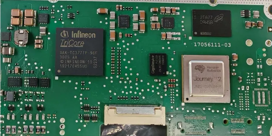
An ADAS radar PCB is a high-frequency automotive circuit board that carries millimeter-wave radar RF paths, antenna structures, radar transceiver routing, power delivery, and reliability controls for driver-assistance sensing modules. In manufacturing, the main challenge is not only making a PCB that is electrically continuous; it is producing a repeatable 76-81 GHz RF structure with stable materials, controlled geometry, documented traceability, and a validation handoff that supports the automotive product approval process.
Key Takeaways
- ADAS radar PCB manufacturing is a process-control problem. At 77/79 GHz, dielectric thickness, copper roughness, etch compensation, solder mask placement, and antenna geometry can all shift RF behavior.
- AEC-Q and ISO 26262 should be treated as system context. A PCB supports component reliability, manufacturing evidence, and functional-safety work products, but the bare PCB does not by itself prove an ASIL target or radar-system compliance.
- Radar boards and EV power boards should not be merged into one design rule. Radar PCBs are dominated by mmWave material and antenna control; EV power PCBs are dominated by high voltage, high current, creepage, clearance, and thermal design.
- PPAP/APQP evidence matters because radar performance depends on repeatability. The release package should identify critical-to-quality features such as RF trace width, dielectric thickness, impedance coupons, antenna dimensions, copper plating, and cleanliness.
- The best RFQ package includes more than Gerbers. Send stackup intent, material callout, controlled-impedance requirements, antenna keepouts, reliability requirements, inspection plan, traceability expectations, and the requested NPI stage.
In This Guide
- What ADAS radar PCB manufacturing is actually controlling
- ADAS radar PCB vs EV power PCB: keep the design routes separate
- Automotive standards context without overclaiming PCB compliance
- 77/79 GHz material and stackup decisions
- Antenna-on-PCB and RF routing manufacturing controls
- Reliability risks in automotive radar PCB production
- Process control, inspection, and traceability
- NPI, APQP, PPAP, and validation handoff
- Common failure modes and prevention controls
- Cost drivers in ADAS radar PCB manufacturing
- RFQ checklist for ADAS radar PCB projects
- Why work with HILPCB
- Reference standards and specifications
- FAQ
What ADAS radar PCB manufacturing controls
ADAS radar PCB manufacturing controls the physical RF structure that allows an automotive radar module to transmit, receive, and process millimeter-wave signals repeatably. The PCB may include antenna-on-PCB arrays, RF feed networks, radar transceiver fanout, power supplies, high-speed digital interfaces, shielding structures, and connector interfaces to the vehicle electronics system.
That definition is deliberately board-level. The PCB is part of the radar sensor, but it is not the complete radar system. The finished module still needs antenna characterization, RF calibration, software, enclosure validation, EMC testing, environmental testing, functional-safety analysis, and vehicle-level integration. A reliable PCB supplier can support those goals by controlling the board features that most strongly affect RF repeatability and automotive durability.
The board-level burden is high because automotive radar often operates around the 76-81 GHz range. At these wavelengths, a trace width shift, dielectric-thickness drift, copper-roughness change, or solder mask mistake can become an RF problem. A board that looks normal under ordinary electrical test can still distort an antenna pattern or add unacceptable insertion loss.
The manufacturing review should therefore answer four questions before release:
| Review question | Why it matters for radar PCB manufacturing | Evidence to prepare |
|---|---|---|
| Which RF material and stackup are frozen? | Dk, Df, copper roughness, thickness tolerance, and CTE affect loss, phase, and reliability | Material datasheet, stackup drawing, resin/copper callout, lamination notes |
| Which geometries are critical-to-quality? | Antenna patches, feed lines, transition zones, and impedance coupons need tighter control than ordinary nets | CTQ list, controlled-net table, antenna drawing, etch-tolerance requirement |
| Which automotive reliability risks must be controlled? | Thermal cycling, humidity bias, vibration, corrosion, CAF, and solder fatigue can create field failures | Reliability plan, cleanliness requirement, coating/sealing assumptions, test matrix |
| Which NPI evidence is required? | Automotive programs need repeatability data, not only a working prototype | APQP/PPAP request, SPC plan, inspection frequency, traceability requirement |
A strong ADAS radar PCB project starts by making those four items visible. Without them, the supplier receives a file package but not the engineering context needed to protect radar repeatability.
ADAS radar PCB vs EV power PCB
ADAS radar PCBs and EV power PCBs often appear together in automotive electronics discussions, but they should not be treated as one design route. They share automotive reliability pressure, documentation expectations, and environmental exposure. Their dominant physical risks are different.
An ADAS radar PCB is usually an RF precision board. Its most sensitive features are the antenna area, RF transmission lines, dielectric thickness, copper profile, solder mask clearance, cavity or shielding interface, and calibration-related repeatability. The main question is whether the fabricated board preserves the electromagnetic structure the radar design expected.
An EV power PCB is usually a high-current and high-voltage reliability board. Its sensitive features are creepage, clearance, copper thickness, via current capacity, insulation system, thermal path, connector strength, and arc or tracking risk. The main question is whether the board can safely carry current and voltage under thermal, mechanical, and environmental stress.
| Area | ADAS radar PCB | EV power / high-voltage PCB | Shared automotive concern |
|---|---|---|---|
| Dominant frequency or energy burden | 76-81 GHz RF and antenna geometry | High current, high voltage, fast switching, heat | EMI/EMC planning and traceability |
| Primary material concern | Low-loss RF laminate, stable Dk/Df, copper roughness | High-Tg, high-CTI, heavy copper, thermal conductivity, insulation | Moisture resistance and thermal cycling |
| Critical geometry | Antenna patch, RF line, GCPW gap, via transition, launch | Creepage, clearance, slot, copper width, thermal via array | Controlled manufacturing tolerance |
| Inspection focus | AOI/AVI, dimensional checks, TDR/VNA coupons when specified, cross-section | Copper thickness, insulation distance, via plating, Hi-Pot at assembly/system level | Process records and lot traceability |
| Validation boundary | RF performance and radar module validation remain system-level | Safety and high-voltage validation remain system-level | PCB supports evidence but does not replace product testing |
This separation avoids a common mistake: using high-voltage safety language to explain radar RF risk, or using mmWave material language to explain EV power risk. A radar board may include power supply sections, and an EV power controller may include communication links, but the design route should follow the dominant failure mechanism.
Automotive standards context
Automotive radar PCB manufacturing sits near several standards and quality systems. Those names are important, but they must be used carefully.
ISO 26262 addresses functional safety for road-vehicle electrical and electronic systems. For a radar program, ISO 26262 can drive requirements for safety mechanisms, diagnostic coverage, failure-mode assumptions, traceability, and verification evidence. A PCB can support this work through manufacturing controls, traceability, separation of safety-related circuits, and stable interconnect implementation. A PCB alone does not prove an ASIL target.
AEC-Q100, AEC-Q101, AEC-Q102, AEC-Q103, AEC-Q104, and AEC-Q200 are component qualification specifications. They apply to ICs, discrete semiconductors, optoelectronic devices, sensors, multichip modules, and passive components, depending on the document. They do not automatically qualify the printed circuit board as an AEC-Q component. The PCB supplier should instead help preserve the conditions needed for qualified components to perform correctly: solderability, thermal path, spacing, cleanliness, mechanical support, and process repeatability.
IATF 16949 is an automotive quality-management-system framework. It is relevant because automotive customers often require disciplined process control, traceability, change control, risk analysis, corrective action, and customer-specific requirements. For a PCB project, this affects how the supplier handles APQP, PPAP, engineering changes, lot records, and special characteristics.
APQP and PPAP are not just paperwork. They are the mechanism for translating a radar design into stable production. For ADAS radar PCB manufacturing, APQP should identify CTQ features early, and PPAP should show that the process can repeatedly produce those features within the agreed control plan.
Standards Boundary at the PCB Level
| Standards term | Safe board-level use | Avoid this overclaim |
|---|---|---|
| ISO 26262 / ASIL | The PCB manufacturing package supports functional-safety evidence and traceability | “This PCB is ASIL-B compliant” without system safety case |
| AEC-Q100 / AEC-Q200 | Components on the BOM may be AEC-qualified; PCB layout and assembly must support their use | “The PCB is AEC-Q100 certified” |
| IATF 16949 | Automotive quality-system context for manufacturing process control | “IATF alone proves radar reliability” |
| PPAP | Customer approval evidence for a stable production process | “PPAP means RF performance is automatically proven” |
| EMC / CISPR / ISO 11452 | Device or module testing context supported by PCB layout and shielding | “Bare PCB passes vehicle EMC” |
This boundary protects both engineering quality and marketing accuracy. It also gives buyers a clearer RFQ: ask for the evidence the supplier can produce, and keep system-level certification with the product owner.
77/79 GHz material and stackup decisions
At 77/79 GHz, material selection is not a purchasing preference. It is part of the RF design. The dielectric constant affects wavelength and antenna geometry. The dissipation factor contributes to insertion loss. Copper roughness affects conductor loss. Thickness tolerance affects impedance and antenna resonance. Dimensional stability affects registration between layers and consistency across production lots.
Common ADAS radar boards use low-loss RF laminates or hybrid stackups that combine a radar RF layer with conventional digital/control layers. A hybrid construction can reduce cost, but it raises lamination and scaling complexity. The manufacturer must understand how each material behaves during pressing, drilling, plating, desmear, etching, and surface finishing.
| Stackup choice | When it may fit | Manufacturing concern |
|---|---|---|
| RF laminate only | Compact radar antenna board with high RF sensitivity | Higher material cost and tighter process windows |
| Hybrid RF + FR-4 stackup | Radar front end combined with digital/control circuitry | Different CTE, resin flow, lamination scaling, and registration behavior |
| Thin RF core for antenna layer | Antenna-on-PCB design needing controlled field geometry | Thickness tolerance and copper roughness become critical |
| Thermoset RF material | Programs seeking lower-loss RF performance with more conventional processing | Validate Dk/Df stability, copper profile, and supplier processing rules |
| PTFE-based RF material | Very low-loss radar or microwave designs | Requires material-specific fabrication controls and process experience |
Material selection should also reflect the final radar architecture. A corner radar, long-range front radar, imaging radar, and short-range side radar may place different emphasis on antenna size, field of view, module packaging, thermal load, and cost. No single laminate is universally best. The better question is which material gives the design enough RF margin while staying manufacturable at the program volume and reliability target.
Practical material review checklist
Before releasing an ADAS radar PCB package, confirm these items:
- RF laminate name, thickness, copper type, and copper roughness assumption.
- Dk and Df values used in electromagnetic simulation, including the frequency and test method basis.
- Stackup drawing with RF layer position, reference planes, prepreg/core thicknesses, and solder mask treatment.
- Lamination scaling expectation for antenna registration and RF feed alignment.
- Surface finish and solder mask restrictions near the RF radiation or transmission structure.
- Whether impedance coupons, RF coupons, or antenna test coupons are required.
- Whether the supplier may substitute an equivalent material only with written approval.
The material decision is strongest when the simulation assumption, stackup drawing, and manufacturing control plan all say the same thing.
Antenna-on-PCB and RF routing manufacturing controls
Many automotive radar modules use antenna-on-PCB structures. That makes the PCB part of the RF aperture rather than just an interconnect carrier. The manufacturer must preserve antenna dimensions, RF feed geometry, and layer registration more tightly than on ordinary automotive boards.
RF routing structures
ADAS radar PCB routing may use microstrip, stripline, grounded coplanar waveguide, substrate-integrated waveguide features, or custom transitions defined by the radar IC vendor. The exact structure depends on the antenna architecture and RFIC package. Manufacturing should not reinterpret these structures casually.
Key features to control include:
- RF trace width and gap.
- Copper thickness after plating.
- Dielectric thickness to reference plane.
- Solder mask opening or mask keepout in the RF area.
- Via fence pitch and via plating quality.
- Launch transition from RFIC or package to the feed network.
- Antenna element dimensions and spacing.
- Board outline and enclosure reference points that affect radome alignment.
The antenna area should be treated as a controlled RF zone. Do not place silkscreen, copper thieving, fiducials, test pads, solder mask, or unnecessary metal in that zone unless the RF designer explicitly approves it.
Etch compensation and copper profile
At mmWave frequencies, conductor shape matters. The width at the top of a trace is not always the width at the bottom, and etch undercut changes the effective geometry. A process that works for ordinary 50-ohm lines at low GHz may not preserve a radar feed network at 77 GHz. The CAM review should therefore confirm etch compensation, copper foil type, and finished-line tolerance before production.
Solder mask and surface finish
Solder mask can change local dielectric loading. In RF antenna areas, the design may require mask-free copper, controlled mask opening, or tightly defined mask clearance. Surface finish can also affect solderability and RF loss; the correct choice depends on the design, assembly process, and corrosion expectations. Avoid changing finish after RF tuning unless the radar team approves the update.
Impedance and RF test coupons
Controlled impedance is useful, but it is not the whole RF answer. A TDR coupon confirms a transmission-line structure under a defined measurement condition. It does not by itself prove antenna radiation pattern, radar range, phase coherence, or module calibration. For higher-risk radar programs, additional RF coupons, VNA measurements, or antenna test structures may be defined by the customer.
Reliability risks in automotive radar PCB production
Automotive radar boards live in a harsh environment: thermal cycling, vibration, moisture, road-salt exposure, cleaning residues, enclosure stress, and long service life. The PCB manufacturing plan must control both RF repeatability and mechanical durability.
Thermal cycling and CTE mismatch
Radar boards often combine copper, RF laminate, prepreg, solder mask, surface finish, components, and enclosure hardware with different coefficients of thermal expansion. Repeated temperature changes can stress plated through holes, microvias, solder joints, and laminate interfaces. Hybrid stackups need special attention because material transitions can concentrate stress.
Humidity, CAF, and ionic contamination
Conductive anodic filament growth and electrochemical migration are major concerns when voltage, moisture, contamination, and glass-fiber paths align. Radar modules may be sealed, but sealed does not mean risk-free. If flux residues, ionic contamination, or moisture ingress remain, insulation resistance can degrade over time. Cleanliness requirements should be explicit in the RFQ.
Vibration and connector stress
A radar module mounted near the bumper, grille, body frame, or chassis must survive vibration and shock. The PCB should avoid creating stress concentration around heavy components, connectors, or mounting holes. If the radar board has a coaxial, board-to-board, press-fit, or high-density connector interface, mechanical support and solder-joint inspection become part of the reliability plan.
Salt spray and corrosion
Salt spray or cyclic corrosion tests are usually module-level or component-level requirements, not a bare-board guarantee. The PCB can support corrosion robustness through surface finish selection, solder mask quality, edge sealing where needed, connector finish selection, cleaning control, and coating strategy when applicable.
| Reliability stress | PCB-level risk | Control method |
|---|---|---|
| Thermal cycling | Via cracking, laminate stress, solder fatigue, RF drift | CTE-aware stackup, plating control, cross-section, thermal validation |
| Humidity bias | CAF, leakage, corrosion, insulation loss | CAF-resistant materials, spacing review, cleanliness control, conformal coating when specified |
| Vibration | Connector fatigue, solder cracking, RFIC or shield stress | Mechanical support, keepout around mounting holes, THT/SMT process control |
| Salt/corrosion | Pad corrosion, connector degradation, conductive residue | Finish selection, cleaning, coating strategy, enclosure coordination |
| Heat from RFIC/processor | Local hot spots, Dk drift, solder fatigue | Thermal vias, copper spreading, thermal interface coordination |
| Manufacturing variation | Antenna pattern shift, insertion-loss variation | SPC, CTQ list, etch control, impedance/RF coupons, traceability |
Process control, inspection, and traceability
ADAS radar PCB manufacturing should be built around special characteristics. These are the features where variation has a disproportionate impact on RF performance, reliability, or customer approval. Typical special characteristics include RF trace width, antenna dimensions, dielectric thickness, copper thickness, registration, via plating, solder mask opening, ionic cleanliness, and impedance.
Process control chain
| Process stage | What can go wrong | Control method |
|---|---|---|
| Material incoming | Wrong laminate, wrong copper foil, lot mismatch | Material certificate, lot traceability, controlled storage |
| Inner-layer imaging | RF geometry shift, registration error | LDI control, AOI, scaling compensation |
| Lamination | Dielectric thickness drift, resin starvation, registration loss | Press recipe control, stackup verification, microsection |
| Drilling / laser drilling | Via position error, smear, rough hole wall | Drill registration checks, desmear control, tool-life management |
| Plating | Insufficient copper, via reliability risk | Plating thickness measurement, cross-section, SPC |
| Etching | RF line width drift, antenna dimension error | Etch compensation, AOI/AVI, line-width measurement |
| Solder mask | Mask intrusion into RF zone, poor registration | Mask keepout checks, inspection against RF zone rules |
| Surface finish | Solderability issue, corrosion risk, RF surface change | Finish thickness control, solderability testing when required |
| Final inspection | Hidden process drift missed | Electrical test, impedance coupon, visual/AOI/AVI, traceability record |
Traceability
Automotive programs need traceability beyond a lot number. The project may require linking a PCB serial or panel ID to material lots, production dates, equipment, operators, lamination press cycle, plating record, AOI result, impedance coupon, microsection, inspection report, and shipment batch. If the board is assembled, traceability may extend to BOM lots, solder paste lots, reflow profiles, X-ray records, programming, and functional-test results.
Traceability is not a substitute for quality. It is the mechanism that lets the team contain a problem quickly if a drift or field issue appears.
NPI, APQP, PPAP, and validation handoff
A radar PCB program should move through staged evidence. The names vary by customer, but the logic is usually the same: prove the concept, lock the design, prove the process, then ramp production.
| Stage | Main purpose | PCB evidence that helps |
|---|---|---|
| EVT / engineering build | Confirm the board can support the intended RF and electrical architecture | Stackup trial, RF/impedance coupons, first article data, DFM notes |
| DVT / design validation | Validate design under environmental, electrical, and mechanical conditions | Reliability samples, cross-sections, material records, cleanliness data |
| PVT / production validation | Confirm the production route can repeat the design | Control plan, SPC data, Run@Rate, inspection frequency, yield data |
| SOP / production | Maintain repeatable output under change control | Traceability, process audits, deviation handling, continuous improvement |
APQP and PPAP content for radar PCBs
For ADAS radar PCB manufacturing, PPAP evidence may include:
- Design records and approved stackup.
- Customer engineering approval when required.
- DFMEA/PFMEA participation or supplier PFMEA.
- Control plan with CTQ features.
- Measurement system analysis for critical dimensions.
- Dimensional report for antenna and RF features.
- Material certificates and laminate lot data.
- Initial process capability for agreed special characteristics.
- Test reports, inspection records, and microsections.
- Appearance approval when relevant.
- Sample parts and master sample.
- Checking aids for coupons or fixtures when applicable.
- Customer-specific requirements.
The exact PPAP level and content should be agreed with the customer. Do not assume that a consumer-electronics NPI package is enough for automotive radar.
Common failure modes and prevention controls
| Failure mode | Likely root cause | Board-level impact | Prevention or detection |
|---|---|---|---|
| Antenna resonance shift | Dielectric thickness drift, Dk mismatch, solder mask change, geometry error | Reduced range, angle error, calibration drift | Material control, RF zone rules, dimensional inspection, RF coupon |
| Excessive insertion loss | High Df material, rough copper, poor transition design, plating variation | Lower radar signal margin | Low-loss material selection, copper profile control, VNA coupon if specified |
| Impedance mismatch | Trace width/gap drift, wrong stackup, dielectric variation | Reflections, phase error, signal distortion | CAM review, TDR coupon, etch SPC |
| CAF or leakage | Moisture, contamination, insufficient spacing, glass/resin path | Intermittent faults or shorts | Cleanliness control, material selection, spacing review, humidity-bias testing |
| Via cracking | CTE mismatch, poor plating, thermal cycling stress | Open circuit, intermittent failure | Plating control, cross-section, thermal cycling validation |
| Solder joint fatigue | Vibration, thermal cycling, heavy connector stress | Intermittent radar module failure | Assembly support, solder-joint inspection, mechanical design review |
| Corrosion at pads/connectors | Salt exposure, poor finish selection, residues, enclosure leak | Increased resistance or failure | Finish selection, coating strategy, cleaning, environmental validation |
| RF zone contamination | Silkscreen, mask bleed, metal near antenna, unapproved copper fill | Pattern distortion or tuning shift | RF keepout rules, CAM lock, final visual inspection |
| Process drift during ramp | Weak SPC, material substitution, uncontrolled scaling | Lot-to-lot RF variation | Control plan, SPC, traceability, change control |
This table is useful during DFM because most radar failures are not caused by one dramatic mistake. They come from small shifts that add up: laminate lot variation, mask registration, trace width, copper roughness, fixture pressure, enclosure alignment, and calibration assumptions.
Cost drivers in ADAS radar PCB manufacturing
ADAS radar PCBs cost more than ordinary automotive boards because the supplier must control RF behavior and automotive reliability at the same time. Cost is driven by material, tolerance, evidence, and risk.
| Cost driver | Why it raises cost | How to manage it |
|---|---|---|
| Low-loss RF laminate | Specialized materials and tighter storage/processing rules | Choose material based on RF margin, not brand prestige alone |
| Hybrid stackup | More complex lamination and scaling control | Freeze stackup early and avoid late material substitution |
| Tight antenna dimensions | Additional AOI/AVI and dimensional checks | Identify antenna CTQs clearly instead of tightening the whole board |
| RF coupons / impedance testing | More panel space and measurement time | Define which coupons are required and how results are judged |
| Automotive traceability | More records and process control | Specify required traceability level early |
| Reliability testing | Samples, time, fixtures, and lab coordination | Separate engineering validation from routine lot release |
| PPAP/APQP documentation | Cross-functional quality work and data collection | Agree PPAP level, special characteristics, and submission timing |
| Turnkey assembly | RFIC, shield, connector, and test complexity | Provide BOM, placement requirements, and functional test plan early |
A lower quote may be risky if it removes the controls that protect radar repeatability. A better cost review asks which controls are critical and which are generic habits carried over from older projects.
RFQ checklist for ADAS radar PCB projects
A complete RFQ package lets the PCB supplier review the design as an RF automotive program, not just as a Gerber job.
Design files
- Gerber or ODB++ data.
- Drill files and controlled-depth requirements.
- Fabrication drawing.
- Assembly drawing if PCBA is requested.
- Netlist and IPC-356 when available.
- 3D model or mechanical outline if enclosure alignment matters.
Stackup and materials
- Approved RF laminate and backup material policy.
- Core/prepreg thicknesses and tolerances.
- Copper type and copper roughness assumption.
- Surface finish requirement.
- Solder mask color and RF-zone keepout rule.
- Controlled-impedance and RF coupon requirements.
RF and antenna information
- Antenna-on-PCB area and keepout.
- RF feed network critical dimensions.
- GCPW/microstrip/stripline structure details.
- Impedance target and measurement method.
- RF coupon or VNA requirement if applicable.
- Restrictions on copper thieving, silkscreen, test pads, and mask in RF zones.
Automotive reliability requirements
- Operating temperature range.
- Thermal cycling or thermal shock expectations.
- Humidity-bias, HAST, salt/corrosion, vibration, or mechanical-shock expectations.
- Cleanliness or ionic contamination requirement.
- CAF requirement if applicable.
- Conformal coating or sealing expectations if PCBA is requested.
Quality and production evidence
- APQP/PPAP level and submission requirements.
- CTQ or special-characteristics list.
- Required SPC data.
- Inspection frequency.
- Microsection requirements.
- Traceability level.
- Change-control expectations.
Assembly and testing
- BOM with automotive-grade component requirements.
- RFIC package, shield, connector, and thermal interface notes.
- Solder paste and reflow constraints.
- X-ray requirements for hidden joints.
- Functional test, programming, or calibration handoff.
- Packaging, ESD, and moisture-control requirements.
Why work with HILPCB
ADAS radar PCB programs need a supplier that treats RF geometry, automotive traceability, and manufacturing evidence as one package. HILPCB supports high-frequency PCB manufacturing, Rogers-material processing, high-speed interconnect review, heavy-copper and thermal PCB routes for power sections, and turnkey PCBA handoff when the project moves from bare board into assembled radar module electronics.
For a radar PCB, HILPCB can review the manufacturability of RF stackups, antenna keepouts, controlled-impedance structures, via transitions, plating requirements, solder mask rules, and special-characteristic inspection planning. For EV power or mixed ADAS/EV control boards, HILPCB can also route the project toward Heavy Copper PCB, High Thermal PCB, or Turnkey Assembly when the dominant risk shifts from RF geometry to current, heat, connector strength, or assembled-board verification.
Relevant HILPCB routes include:
Send the stackup draft, RF material callout, Gerber or ODB++ package, and PPAP or validation expectations before fabrication. That is the fastest way to identify RF-zone manufacturing risks before they become late-stage calibration or yield problems.
Reference standards and specifications
- ISO 26262 — Road vehicles — Functional safety
- IATF 16949 — Automotive quality management system requirements
- AEC-Q100 — Failure mechanism based stress test qualification for integrated circuits
- AEC-Q101 — Failure mechanism based stress test qualification for discrete semiconductors
- AEC-Q102 — Failure mechanism based stress test qualification for optoelectronic semiconductors
- AEC-Q103 — Failure mechanism based stress test qualification for sensors
- AEC-Q104 — Failure mechanism based stress test qualification for multichip modules
- AEC-Q200 — Stress test qualification for passive components
- IPC-6012DA — Automotive applications addendum to IPC-6012
- IPC-A-600 — Acceptability of printed boards
- IPC-A-610 — Acceptability of electronic assemblies
- IPC-TM-650 — Test methods manual
- IEC 60068 — Environmental testing
- CISPR 25 — Vehicles, boats and internal combustion engines — Radio disturbance characteristics
- ISO 11452 — Road vehicles — Component test methods for electrical disturbances from narrowband radiated electromagnetic energy
- ETSI EN 302 264 — Short range radar equipment operating in the 77 GHz to 81 GHz band
- ITU-R M.2057 — Systems characteristics of automotive radars operating in the frequency band 76-81 GHz
FAQ
What is the main manufacturing challenge in an ADAS radar PCB?
The main challenge is preserving RF geometry and material behavior repeatably. At 77/79 GHz, small variation in dielectric thickness, copper roughness, trace width, solder mask location, or antenna dimensions can affect impedance, loss, and antenna behavior.
Is an ADAS radar PCB automatically ISO 26262 or ASIL compliant?
No. ISO 26262 and ASIL targets belong to the vehicle or item-level functional-safety process. A PCB can support the safety case through traceability, process control, reliable interconnect, separation, and documented manufacturing evidence, but the bare PCB does not prove ASIL compliance by itself.
Do AEC-Q100 and AEC-Q200 apply to the PCB?
AEC-Q100 and AEC-Q200 are component qualification documents for ICs and passive components. They are relevant to the BOM and automotive reliability context, but they should not be described as direct PCB certifications.
Why does antenna-on-PCB make radar boards harder to fabricate?
Antenna-on-PCB turns the board into part of the RF radiator. The antenna area, feed network, dielectric thickness, copper profile, and mask keepout must match the electromagnetic design. Unapproved copper, silkscreen, solder mask, or dimensional drift can shift the RF response.
What is the difference between an ADAS radar PCB and an EV power PCB?
An ADAS radar PCB is dominated by mmWave RF material, antenna geometry, and signal integrity. An EV power PCB is dominated by high voltage, high current, thermal path, creepage, clearance, and insulation reliability. Some automotive modules contain both concerns, but the manufacturing route should follow the dominant risk.
What should be included in an ADAS radar PCB RFQ?
Include Gerber or ODB++ files, stackup, RF laminate callout, controlled-impedance requirements, antenna keepouts, copper roughness assumption, surface finish, reliability expectations, APQP/PPAP level, inspection requirements, traceability expectations, and assembly/test needs if PCBA is requested.
Can HILPCB help with both radar RF boards and EV power electronics boards?
Yes. HILPCB can route radar projects through high-frequency and Rogers-material PCB review, and power electronics projects through heavy copper, high thermal PCB, and turnkey assembly review. The first step is to identify whether the dominant risk is RF repeatability, high current, high voltage, thermal stress, or assembled-board validation.
Next steps
If your radar design is already tied to a 77/79 GHz antenna-on-PCB structure, do not wait until after the first build to clarify material, stackup, antenna keepout, impedance coupon, and traceability requirements. Those details determine whether the prototype is a meaningful RF validation vehicle or only a mechanically correct board.
Send your Gerber or ODB++ package, RF stackup, laminate callout, antenna keepout drawing, and requested PPAP or reliability expectations to [email protected], or upload the files through the Quote page. HILPCB will review the RF-zone manufacturability, high-frequency material route, and production evidence requirements before fabrication.