
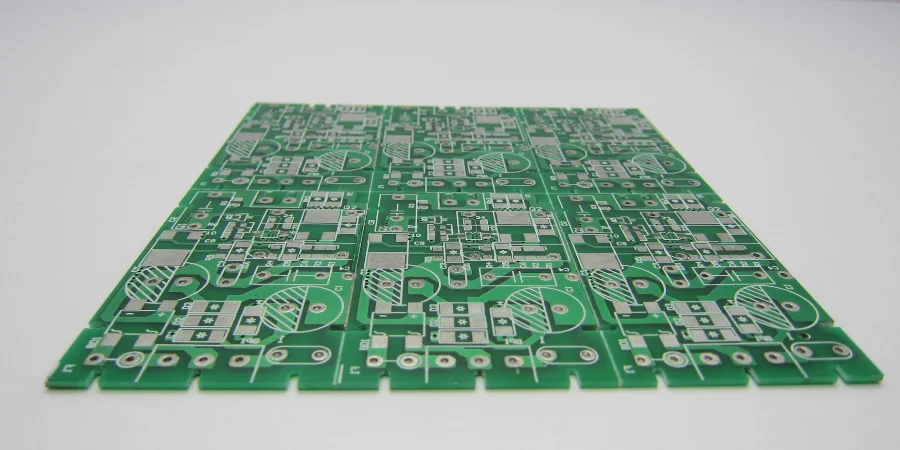
In the world of modern electronics, the Double-Sided Printed Circuit Board (PCB) stands as one of the most versatile and cost-effective foundational components. More than just a bridge connecting electronic parts, it serves as the bedrock of product performance and reliability. Therefore, choosing a skilled and dependable double-sided-pcb-manufacturer is vital for the success of any electronics project.
This guide delves into the core knowledge surrounding double-sided PCBs, dissecting their complex manufacturing processes in detail, and providing you with crucial criteria for selecting an exceptional manufacturer.
1. What is a Double-Sided PCB? Why is it Central to Electronics?
A Double-Sided PCB, as the name suggests, is a circuit board featuring conductive copper layers on both the top and bottom surfaces of an insulating substrate. This substrate is most commonly FR-4 PCB material. The defining feature setting it apart from the products in our single-double-layer PCB category is the Plated Through Hole (PTH), a critical technology enabling electrical connections between layers.
The Plated Through Hole (Via) is a small hole drilled through the PCB, with its inner wall coated with a layer of metal copper through chemical and electroplating processes. This forms a conductive channel, allowing circuit traces to "jump" across physical space and conduct freely between the two layers.
Key Advantages of Double-Sided PCBs:
- Higher Routing Density: Boasting two routing layers, it enables designers to achieve more complex circuit connections within a limited space, significantly reducing product size.
- Superior Design Flexibility: It addresses the challenge of intersecting traces found in single-sided boards, simplifying circuit layout design and shortening R&D cycles.
- Optimized Electrical Performance: The capability to establish complete ground and power planes effectively lowers impedance, minimizes signal interference, and enhances circuit stability and performance.
- Excellent Cost-Effectiveness: Compared to more intricate multilayer PCBs, double-sided boards meet the needs of the majority of applications while delivering a competitive cost.
2. In-Depth Analysis of the Double-Sided PCB Manufacturing Process
A top-tier double-sided-pcb-manufacturer must possess precise control over the manufacturing process. The creation of a double-sided PCB is significantly more complex than that of a single-sided board, with the core being the realization of the PTH. Here's a detailed breakdown of the mainstream manufacturing process within the industry.
2.1 Pattern Plating Process – The Standard Approach
This is the most classic and well-established method for manufacturing double-sided PCBs. For applications requiring operation in high-temperature environments, a high-TG PCB material may be specified.
Base Material/Copper Clad Laminate → Cutting → CNC Drilling → Desmearing/Hole Wall Activation → Chemical Copper Deposition (PTH) → Full Board Thin Copper Plating → Imaging Transfer (Applying Dry Film or Wet Film) → Exposure & Development → Pattern Plating (Copper & Tin/Lead) → Film Removal → Etching → Tin/Lead Removal → Inspection & Repair → Solder Mask → Legend/Silkscreen → Surface Finish (e.g., HASL, ENIG) → Profiling (CNC Routing/V-Cut) → Electrical Testing (Flying Probe or Test Jig) → Final Quality Control (FQC) → Vacuum Packaging → Product Shipment
- Key Steps Interpreted:
- CNC Drilling: Precisely drills all conductive and mounting holes, with accuracy directly affecting the subsequent PTH quality.
- Chemical Copper Deposition (PTH): Chemically deposits a micron-thin layer of conductive copper onto the insulated hole walls, marking the first step in achieving interlayer conduction and serving as the heart of the entire process.
- Pattern Plating: Selectively thickens copper plating only on traces and hole walls intended to be retained, forming a sufficient conductive copper thickness and plating with an etch-resistant tin/lead alloy.
- Etching: Removes excess copper foil not protected by the tin/lead plating, forming the final circuit pattern.
- Solder Mask: Covers the board with an insulating protective layer (typically green), shielding traces from oxidation and soldering shorts, exposing only the pads requiring soldering.
2.2 Solder Mask on Bare Copper (SMOBC) Process
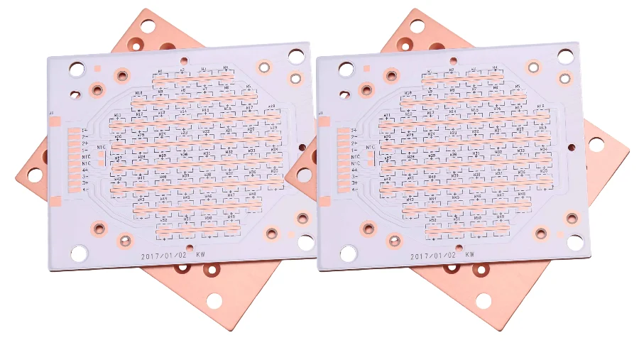
SMOBC is a mainstream precision double-sided board manufacturing process that developed in the 1980s. Its main advantage lies in resolving solder bridging shorts between fine-pitch traces while providing superior solderability and storage properties. This process is essential for manufacturing more advanced boards like HDI PCBs.
SMOBC (Pattern Plating Followed by Lead-Tin Removal) Process Flow:
Double-Sided Copper Clad Laminate → ... (Same as Pattern Plating Process, up to Completion of Etching) ... → Lead-Tin Removal → Inspection → Cleaning → Application of Solder Mask → Nickel/Gold Plating for Plugs (If Applicable) → Hot Air Solder Leveling (HASL) or Electroless Nickel Immersion Gold (ENIG) and Other Surface Finishes → Cleaning → Silkscreen Printing → Profiling → Cleaning & Drying → Final Product Inspection → Packaging & Shipping
- Difference from the Standard Process: This process includes a "Lead-Tin Removal" step after etching, allowing the solder mask to be directly applied to the bare copper traces instead of being applied over tin/lead.
2.3 Plugging Via SMOBC Process
This process is critical in specific applications (such as vias under BGA pads), designed to prevent solder paste from flowing into the vias during soldering. For applications with high current demands, a heavy copper PCB might be needed.
Double-Sided Copper Clad Laminate → Drilling → Chemical Copper Deposition → Full Board Copper Plating → Via Plugging (Filling Holes with Specialized Ink) → Imaging Transfer (Positive Film) → Etching → Removal of Plugging Material/Ink → Cleaning → Solder Mask Application → ... (Subsequent Steps Same as SMOBC Process) ... → Finished Product
- Process Core: The key lies in the perfect filling of the holes and subsequent planarization, ensuring reliable soldering and solder mask application.
3. Single-Sided PCB vs. Double-Sided PCB: Comparing Core Differences
| Feature | Single-Sided PCB | Double-Sided PCB |
|---|---|---|
| Conductive Layers | Copper traces on one side of the substrate only. | Copper traces on both sides of the substrate. |
| Interlayer Connection | None; holes are for component mounting only (non-conductive). | Achieved through Plated Through Holes (PTH) for connecting circuits on both sides. |
| Routing Complexity | Extremely Low; routing cannot intersect and is heavily restricted. | Medium to High; more flexibility with vias for layer changes, higher routing density possible. |
| Manufacturing Process | Simple; lacks PTH and secondary plating processes. | Complex; relies on PTH process, with longer workflows and stringent control requirements. |
| Cost | Lowest. | Moderate; represents an optimal balance between performance and cost. |
| Application Areas | Simple electronics like calculators, remote controls, and power boards. | Vast majority of consumer electronics, industrial controls, communication devices, and automotive electronics. |
4. SMT (Surface Mount Technology) Assembly Considerations for Double-Sided PCBs
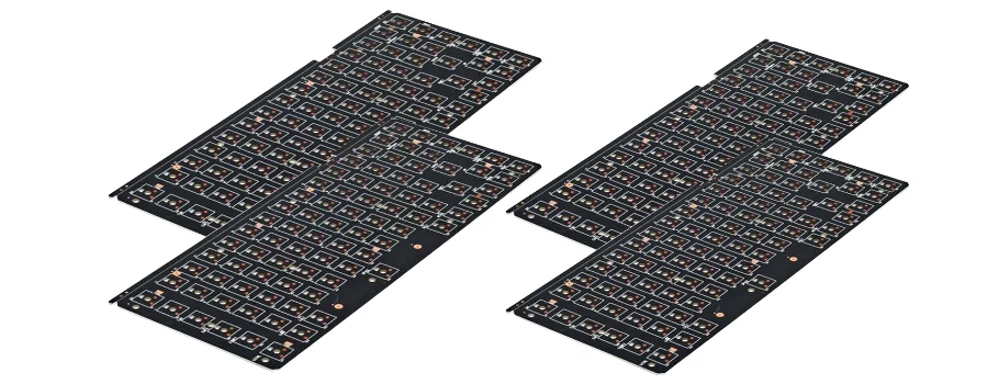
With components on both sides, SMT assembly for double-sided PCBs places higher demands on the double-sided-pcb-manufacturer's process control.
- Two-Pass Reflow Challenges:
- First-Side Soldering: Initially solder the side with fewer or smaller components, or the side demanding greater planarity (e.g., the side with BGA or QFN chips).
- Second-Side Soldering: Flip the PCB, apply solder paste, and mount the second side's components. At this point, the components on the first side will be upside down and pass through the high-temperature reflow oven again.
- Critical Process Control Points:
- Component Placement: Heavier or larger components should be placed on the second side to be soldered to prevent them from falling off during the second reflow process.
- Temperature Resistance: Components on the first side must withstand the thermal shock of at least two high-temperature reflow soldering cycles.
- Board Warpage: After the first high-temperature pass, the PCB may undergo minor warping, affecting the solder paste printing accuracy on the second side. Experienced manufacturers control warpage by optimizing the oven temperature profile and using high-quality base materials.
- Through-Hole Components (PIP/THT): If the pins of reflow-soldered through-hole components are too long, they may interfere with the planarity of the stencil for the second side's solder paste printing, requiring special attention during design.
5. How to Select a Professional Double-Sided PCB Manufacturer
Choosing the wrong supplier can lead to project delays, cost overruns, and even product failure. When evaluating a double-sided-pcb-manufacturer, focus on the following core elements:
- Process Capabilities and Technical Specifications: Confirm that their minimum trace width/spacing, minimum hole diameter, board thickness tolerance, and other process capabilities meet your design requirements.
- Quality System Certifications: Do they have international quality management system certifications like ISO 9001? Do they adhere to IPC industry standards for production and inspection?
- Process Control Capabilities: Do they have strict Statistical Process Control (SPC) and monitoring systems for critical processes like PTH, plating, and etching?
- DFM (Design for Manufacturability) Support: An excellent manufacturer will provide a professional DFM review report before production to help you optimize your design, reduce costs, and mitigate production risks.
- Testing Equipment and Capabilities: Are they equipped with advanced testing equipment like Automated Optical Inspection (AOI) and Flying Probe Testers to ensure that every PCB shipped is 100% qualified?
- Customer Service and Responsiveness: Do they have a professional engineering team to quickly address your technical questions? Is the delivery cycle stable and transparent? Can they provide turnkey assembly or SMT assembly services for a complete solution?
Conclusion
Double-sided PCBs are the backbone of modern electronics. A deep understanding of the complexities and key control points in their manufacturing process, along with the ability to select a technically proficient, quality-assured, and service-oriented double-sided-pcb-manufacturer, is the most critical guarantee for ensuring your product successfully transitions from design blueprints to the market.
FAQ About Double Sided PCB Manufacturers
Q1: What design files do I need to send to a Double Sided PCB Manufacturer for a fast quote?
Typically you should provide: Gerber or ODB++ files, NC drill file, board outline, stack-up/material requirements (e.g. FR-4, high-Tg), fabrication notes (min track/space, copper weight, finish), and an assembly drawing if you need assembly. For a full PCBA quote, add a complete BOM and pick-and-place file. Zipping everything into one archive helps any double sided PCB manufacturer respond faster.
Q2: How can I fairly compare prices from different Double Sided PCB Manufacturers?
Make sure every double sided PCB manufacturer is quoting the same specs: layer count, material, copper thickness, finish, solder mask, panelization, and test requirements. Ask them to separate NRE/tooling, bare board cost, and assembly cost, and request several quantity breaks (e.g. 10/100/1000 pcs) to see which double sided PCB fabrication partner scales best with your volume.
Q3: What are typical lead times and MOQs for a Double Sided PCB Manufacturer?
For most double sided PCB manufacturers: prototypes are about 3–7 working days for bare boards and 7–15 days for assembled boards; standard production is usually 10–20 days depending on complexity. MOQs can start as low as 5–10 pcs for prototype-oriented suppliers and go much higher for mass-production double sided PCB manufacturers.
Q4: Should I choose a local or overseas Double Sided PCB Manufacturer?
Local double sided PCB manufacturers offer easier communication, faster shipping, and simpler on-site audits. Overseas manufacturers often provide lower unit prices and strong capacity for high-volume double sided PCB fabrication and assembly. A common strategy is to use a local supplier for early prototypes, then add a vetted offshore double sided PCB manufacturer for cost-optimized volume.
Q5: What quality standards should a Double Sided PCB Manufacturer meet?
Look for a double sided PCB manufacturer that works to IPC-6012 and IPC-A-600/610, and holds certifications such as ISO 9001 (basic quality), plus IATF 16949 or ISO 13485 for automotive or medical markets. For high-reliability double sided PCB manufacturing, also check they can provide controlled-impedance data, hole-wall thickness reports, solderability tests, and 100% electrical test records.