
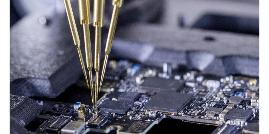
Modern PCB programs fail for more reasons than visible solder defects. A board can look clean after AOI and still contain an open via, a copper short, a swapped component, a marginal BGA connection, a wrong impedance structure, or a power rail that collapses only under load. That is why PCB electrical testing should be planned as a test strategy, not treated as a final checkbox.
For HILPCB customers, the key question is not simply “Can this board be electrically tested?” The better question is: what level of electrical evidence does this design need before it moves to assembly, system integration, or mass production?
This guide separates the major test layers used in PCB and PCBA manufacturing:
- bare board continuity and isolation testing before assembly
- flying probe testing for prototypes and low-volume builds
- fixture-based ICT for repeatable production screening
- boundary scan for dense digital assemblies with limited probe access
- controlled impedance and high-speed signal validation
- Hi-Pot, insulation resistance and leakage checks for high-voltage designs
- functional test and test-data traceability for PCBA release
The goal is to help engineering, quality and sourcing teams choose the right test coverage without overclaiming what any single test can prove.
Key takeaways
- Electrical test is not one method. Bare board E-test, flying probe, ICT, boundary scan, impedance testing and functional test each find different defect classes.
- Bare board testing protects the build before components are mounted. It confirms net continuity and isolation, but it does not validate component behavior, solder joints or system performance.
- PCBA testing needs design-for-test input. ICT, boundary scan and functional test are much stronger when test points, JTAG chains, programming access and fixture constraints are considered before layout release.
- Controlled impedance testing is not the same as full signal-integrity validation. TDR coupons can confirm stackup and process consistency, while eye diagrams, VNA measurements and protocol tests address system-level behavior.
- High-voltage and safety-related boards need explicit acceptance criteria. Hi-Pot, insulation resistance and leakage testing must follow the end-product requirements, not generic marketing claims.
- Traceability matters. Good electrical test data should be tied to lot, panel, board serial number, fixture, program revision and failure disposition.
In this guide
- What PCB electrical testing actually verifies
- Bare board electrical testing before assembly
- Flying probe, ICT and boundary scan for PCBAs
- Controlled impedance and high-speed signal validation
- Hi-Pot, insulation resistance and high-voltage checks
- Functional testing, fixtures and traceability
- Common electrical test failures
- Cost drivers and RFQ checklist
- Reference standards and test frameworks
- FAQ
What PCB electrical testing actually verifies
PCB electrical testing verifies whether the manufactured board or assembled PCBA behaves electrically according to a defined test plan. That definition is important. Testing does not prove that a design is perfect, that a product is certified, or that a system will pass every field condition. It provides evidence against specific failure modes.
A strong electrical test plan starts by separating bare board defects from assembled board defects and system-level performance risks.
Bare board testing checks the fabricated PCB before components are mounted. It looks for opens, shorts, incorrect net connectivity, excessive resistance, isolation failures and sometimes controlled impedance deviation. This step is critical because once the PCB is assembled, an internal layer open or copper short becomes much harder and more expensive to diagnose.
PCBA testing checks the assembled electronics. It can verify component placement, values, power rails, programming, BGA connectivity, digital interconnects, sensor inputs, communication interfaces and functional behavior. However, PCBA testing depends heavily on test access. If the layout has no test pads, no programming header, no boundary-scan chain and no fixture strategy, even excellent equipment will have limited coverage.
High-speed and high-voltage testing add another layer. A high-speed PCB may need controlled impedance coupons, TDR checks, eye diagram validation, jitter review, VNA measurements or protocol testing. A power or isolation board may need Hi-Pot, insulation resistance, leakage and creepage/clearance review. These tests should be tied to the design risk, not copied from a generic checklist.
The table below shows how the major test categories fit together.
| Test layer | Typical timing | What it verifies | What it does not prove |
|---|---|---|---|
| Bare board E-test | After PCB fabrication, before assembly | Net continuity, isolation, opens, shorts, resistive defects | Component behavior, solder joint quality, firmware, system performance |
| Controlled impedance test | PCB fabrication stage, usually on coupons | Stackup and trace geometry consistency for controlled nets | Full channel behavior, connector launch quality, protocol compliance |
| Flying probe | Prototype or low-volume PCBA | Nets, component values, some powered checks without custom fixture | High-throughput production coverage, full dynamic system behavior |
| ICT | Medium/high-volume PCBA with fixture | Component values, opens/shorts, solder defects, programming support | Real end-use behavior unless paired with functional test |
| Boundary scan | Dense digital PCBA with JTAG-capable ICs | Interconnects around BGAs and dense digital devices | Analog behavior, non-JTAG devices, poor chain design |
| Functional test | After assembly and programming | Real operating modes, power sequencing, communication, sensors, outputs | Root cause of every failure unless paired with diagnostic coverage |
| Hi-Pot / IR / leakage | High-voltage or safety-related boards | Isolation strength, insulation resistance, leakage behavior under defined conditions | End-product safety certification by itself |
Electrical testing becomes most valuable when these layers are planned together. A board does not need every test in every case, but every test that is required should have clear acceptance criteria, fixture assumptions and data ownership.
Bare board electrical testing before assembly
Bare board electrical testing is the first major quality gate after PCB fabrication. At this stage, the board has no components, so the goal is straightforward: confirm that the copper network matches the customer-supplied netlist and that isolated nets remain isolated.
For simple boards, this may sound routine. For multilayer, HDI, fine-pitch or high-current boards, it is essential. Inner-layer opens, via plating defects and copper residues may not be visible after lamination. Electrical test is often the only practical way to screen those defects before assembly cost is added.
Continuity testing
Continuity testing confirms that all points belonging to the same net are electrically connected within the defined resistance limit. It helps catch:
- open traces
- incomplete via plating
- broken inner-layer connections
- damaged pads
- routing or CAM errors
- resistive connections caused by marginal copper or plating defects
For high-current designs, continuity should not be treated as a simple yes/no condition. A connection can pass a basic continuity check and still have excessive resistance for the intended current. For heavy copper PCBs, busbar-adjacent boards, motor-drive boards and power converters, resistance limits should be defined with the expected current path in mind.
Isolation testing
Isolation testing confirms that nets which should remain separate do not have unintended copper bridges, conductive contamination or insufficient insulation. It helps catch:
- copper shorts
- etching residues
- soldermask or fabrication contamination
- spacing violations
- laminate or via defects that reduce insulation margin
Isolation is especially important for high-voltage, medical, industrial, solar, battery and power electronics designs. A low-voltage logic board may only need basic isolation screening, while a high-voltage board may require a much more specific insulation test plan.
Fixture test vs flying probe for bare boards
Bare board electrical testing is usually performed by fixture or flying probe.
A fixture test is fast and repeatable once tooling is made. It is cost-effective for volume production, but fixture setup cost and lead time make it less attractive for prototypes or frequent design revisions.
Flying probe testing is slower, but it does not require a dedicated fixture. It is well suited for prototypes, engineering samples, low-volume builds and designs that are still changing.
| Method | Best fit | Strength | Limitation |
|---|---|---|---|
| Flying probe bare board test | Prototype, small batch, changing designs | No fixture cost, fast setup, flexible netlist changes | Slower cycle time for volume production |
| Fixture-based bare board test | Stable design, higher volume | Fast cycle time, repeatable production screening | Tooling cost and fixture lead time |
| Combination strategy | NPI to mass production | Flying probe early, fixture later | Requires test strategy update as design matures |
What HILPCB needs for bare board electrical test
To avoid ambiguity, send the complete fabrication package with:
- Gerber or ODB++ data
- IPC-356 netlist when available
- stackup and copper weight
- controlled impedance requirements
- high-voltage spacing or isolation requirements
- plated slot, castellated edge or edge connector requirements
- test report requirements, if your customer needs a specific format
When the netlist and design intent are clear, electrical testing becomes a controlled manufacturing step instead of a best-effort inspection.
Flying probe, ICT and boundary scan for PCBAs
Once the PCB is assembled, electrical testing becomes more complex. The test must verify not only the copper network but also component placement, solder joints, power sequencing, programming and functional behavior.
There is no single best PCBA test method. The right choice depends on volume, board density, component package style, test access and product risk.
Flying probe testing for PCBA prototypes
Flying probe testing uses movable probes to contact pads, test points and component terminals without a custom bed-of-nails fixture. It is valuable during prototype and low-volume builds because the program can be created or modified more quickly than a fixture.
Flying probe can help detect:
- opens and shorts
- missing or wrong components
- resistor and capacitor value errors
- diode polarity mistakes
- some connector and netlist defects
- limited powered measurements, depending on fixture and access
Its limitation is throughput. Flying probe is usually not the best primary test method for high-volume production, but it is highly useful in early NPI because it can catch layout, BOM and assembly issues before fixture investment.
In-circuit testing
ICT uses a custom test fixture to contact many points on the PCBA at once. It is usually more economical when volumes justify fixture cost. ICT can provide strong diagnostic coverage for component-level defects, but it must be designed into the PCB.
ICT works best when the layout includes:
- accessible test points on important nets
- stable probe landing pads
- enough spacing for fixture pins
- fixture-friendly board support
- programming access for MCUs, FPGAs or memory
- clear power rail segmentation
- known no-test nets and accepted coverage gaps
ICT can check component values, opens, shorts, incorrect parts, orientation issues, and sometimes perform programming or limited powered tests. It cannot magically test nets that have no access. For dense HDI boards, BGA-heavy assemblies or very small form factors, ICT coverage may need to be supplemented with boundary scan and functional test.
Boundary scan for dense digital boards
Boundary scan, commonly associated with IEEE 1149.1 / JTAG, is especially valuable when physical probing is difficult. It allows supported ICs to help test interconnects between devices, which is useful for BGA packages, fine-pitch digital buses and dense assemblies.
Boundary scan can support:
- digital interconnect testing
- BGA solder joint screening
- memory interface checks, depending on device support
- programming and configuration
- debug access during NPI
- partial test coverage when ICT access is limited
Boundary scan has limits. It requires compatible devices, a planned chain, correct pull resistors, accessible TAP signals and a test strategy. It does not replace analog measurement, power rail validation, RF test or full functional testing. It should be designed into the board from the beginning.
| PCBA method | Best use case | Main advantage | Main limitation |
|---|---|---|---|
| Flying probe | Prototype and low-volume PCBA | Low setup cost, flexible program changes | Slower for volume, limited dynamic test capability |
| ICT | Medium/high-volume PCBA | Fast and repeatable component-level screening | Requires fixture and DFT access |
| Boundary scan | Dense digital PCBA and BGA-heavy designs | Tests digital interconnects without direct physical access | Requires JTAG-capable devices and planned chain |
| Functional test | Final product behavior | Confirms real operating modes | Often slower and less diagnostic unless carefully designed |
Controlled impedance and high-speed signal validation
High-speed boards need more than continuity and isolation. A board can be electrically connected and still fail because the signal path has too much loss, reflection, crosstalk, skew or impedance discontinuity.
This is where controlled impedance testing and high-speed validation become important.
Controlled impedance testing
Controlled impedance testing usually uses a TDR method on test coupons fabricated on the same panel as the production boards. The coupon represents the intended trace structure: microstrip, stripline, differential pair, coplanar waveguide or another controlled geometry.
The purpose is to verify that the actual fabricated stackup and trace geometry are close enough to the design target. It helps detect:
- dielectric thickness deviation
- trace width deviation
- copper plating changes
- etch compensation issues
- lamination variation
- material lot variation
Controlled impedance testing is especially important for:
- PCIe, USB, HDMI, MIPI, Ethernet and SerDes boards
- RF and microwave boards
- memory interfaces
- optical module PCBs
- backplanes and connector-heavy systems
- high-speed HDI PCBs
However, impedance coupon results are not the same as full channel validation. They do not automatically prove that connectors, vias, package launches, cables, equalization and protocol margins are acceptable. They confirm manufacturing consistency for the controlled structures being tested.
Eye diagram, jitter and BER validation
For high-speed digital systems, the next level of validation may include eye diagrams, jitter measurement, bit error rate testing and protocol compliance testing. These are usually performed at the assembly or system level rather than as a bare board production test.
This type of validation is important when the risk is not just geometry, but real data transmission quality.
Examples include:
- PCIe links between CPU, FPGA, retimer or connector
- Ethernet links in switches and optical modules
- MIPI camera/display links
- high-speed backplanes
- RF transceiver data paths
- storage and memory interfaces
VNA and S-parameter testing
For RF, microwave, mmWave and very high-speed interconnects, VNA measurement may be required to characterize insertion loss, return loss, phase, crosstalk and de-embedded channel behavior. This is common in high-frequency PCB, antenna modules, optical module boards and backplane work.
S-parameter testing should be planned carefully because fixtures, launches and calibration method can dominate the result. If the test setup is not designed correctly, the measurement may show fixture problems rather than board problems.
| Test type | Usually answers | Typical output |
|---|---|---|
| TDR impedance coupon | Did fabrication hold the intended impedance structure? | Single-ended or differential impedance report |
| Eye diagram | Does a real digital link have enough timing and voltage margin? | Eye height, eye width, jitter metrics |
| BER test | Does the link maintain low error rate under defined conditions? | Pass/fail and error statistics |
| VNA / S-parameter test | What is the RF or high-speed channel behavior? | Insertion loss, return loss, phase, crosstalk |
| Protocol compliance test | Does the assembled product meet the interface test suite? | Interface-specific compliance report |
Hi-Pot, insulation resistance and high-voltage checks
Electrical testing is not only for high-speed boards. High-voltage boards need their own strategy: insulation, leakage and dielectric withstand behavior.
This matters for industrial power supplies, renewable-energy inverters, battery systems, EV charging hardware, medical equipment, LED drivers and any board where hazardous voltage may be present.
Hi-Pot testing
Hi-Pot testing applies a defined high voltage between isolated circuits to check whether insulation can withstand the stress without breakdown. The actual voltage, ramp time, dwell time, trip current and test points must come from the end-product safety design and customer requirement.
A PCB supplier should not invent Hi-Pot conditions. The correct values depend on:
- working voltage
- insulation category
- pollution degree
- altitude
- material group
- creepage and clearance
- product safety standard
- customer risk assessment
Insulation resistance testing
Insulation resistance testing measures resistance between isolated conductive features under a defined voltage. It is useful for detecting contamination, moisture sensitivity, inadequate spacing, dielectric defects and leakage paths.
For boards exposed to humidity, condensation, dust, flux residue or outdoor environments, insulation testing may need to be paired with cleaning controls, ionic contamination controls and coating validation.
Leakage current and product-level testing
Leakage current is usually a product-level safety measurement, not a bare PCB claim. The PCB can support low leakage through spacing, routing, material selection, coating windows and cleanliness, but final leakage depends on the entire power architecture, components, enclosure, wiring and grounding scheme.
For HILPCB, the safe and useful role is to manufacture and test according to the provided high-voltage requirement, then document the results with clear traceability.
Functional testing, fixtures and traceability
Functional testing verifies that the assembled board operates in the intended way. It may be simple, such as power-on current and LED response, or complex, such as firmware loading, sensor simulation, motor output, RF transmission, Ethernet traffic and thermal monitoring.
A good functional test should answer three questions:
- Does the board power up safely?
- Does it communicate and respond correctly?
- Does it meet the critical operating limits defined for release?
Fixture design
Functional test fixture design is often underestimated. A poor fixture can create false failures, intermittent contact, unstable power, poor grounding or misleading measurements.
A production-ready fixture should consider:
- stable board support and alignment
- repeatable connector engagement
- protected power input
- current limiting and fault shutdown
- programming access
- calibration references
- ESD protection
- thermal conditions if the board dissipates significant power
- fixture self-test and maintenance plan
For RF or high-speed boards, fixture design also needs controlled impedance launches, short signal paths and calibration/de-embedding plans.
Test coverage
Test coverage should be discussed before layout release, not after the first boards arrive. Engineering and manufacturing teams should identify:
- critical nets that must be probed
- power rails that must be measured
- safety-related signals
- programming and boot-mode access
- boundary-scan chain coverage
- component classes that cannot be tested directly
- acceptable no-test areas
- functional outputs that require external loads or simulators
Coverage is not only about reaching 100 percent of nets. The more useful metric is whether the test plan detects the most important manufacturing and assembly risks for the specific product.
Traceability and failure disposition
Electrical test data becomes more valuable when it is tied to manufacturing history. For production programs, test records should identify:
- board serial number or panel ID
- test program revision
- fixture ID
- operator or station
- date and time
- pass/fail result
- measured values for critical parameters
- failure code and repair action
- retest result
- lot and material traceability, when required
This supports root-cause analysis, customer reporting and continuous improvement. It also avoids the common problem of having a pass/fail result with no diagnostic value.
Common electrical test failures
The most common electrical test failures are not dramatic. They are usually small manufacturing or assembly issues that become expensive only if they escape.
| Failure mode | Where it appears | Likely cause | Detection method | Prevention |
|---|---|---|---|---|
| Open net | Bare board or PCBA | Broken trace, via plating issue, solder joint open | Bare board E-test, ICT, flying probe, boundary scan | Netlist test, via quality control, DFM review |
| Short between nets | Bare board or PCBA | Etch residue, solder bridge, component misplacement | Isolation test, ICT, flying probe | Spacing review, solder paste control, AOI |
| High resistance connection | Bare board or power PCBA | Marginal plating, weak solder, damaged via | Resistance test, powered load test, thermal imaging | Plating control, solder process control, current-path review |
| Wrong component value | PCBA | BOM, feeder or placement error | ICT, flying probe, functional test | BOM control, feeder verification, AOI |
| BGA interconnect defect | Dense PCBA | Head-in-pillow, open ball, bridge, void issue | X-ray, boundary scan, functional test | Reflow profile control, package handling, DFM |
| Impedance deviation | High-speed/RF PCB | Stackup, etch or material variation | TDR coupon, VNA in advanced cases | Stackup lock, impedance coupons, material control |
| Power rail droop | PCBA functional test | PDN weakness, wrong regulator, solder defect | Functional test, oscilloscope, load transient test | PDN review, decoupling plan, layout review |
| Hi-Pot failure | High-voltage PCB/PCBA | Spacing issue, contamination, dielectric defect | Hi-Pot, insulation resistance | Creepage/clearance review, cleanliness control |
| Intermittent failure | PCBA or system test | Connector issue, cracked joint, fixture contact | Thermal cycling, vibration, repeated functional test | Connector strain relief, fixture maintenance, solder control |
| False test failure | Test station | Fixture wear, poor contact, unstable power | Golden board check, fixture self-test | Fixture PM, calibration, station validation |
Cost drivers and RFQ checklist
Electrical testing cost depends on the type of board, required coverage, test time, tooling and documentation. A simple bare board continuity/isolation test is very different from a PCBA program that needs ICT, boundary scan, firmware programming, functional load testing and serialized reports.
Main cost drivers
| Cost driver | Why it affects price |
|---|---|
| Board density | More nets and fine-pitch access increase program complexity |
| Production volume | Fixture cost is easier to justify at higher volume |
| Test method | Flying probe, ICT, boundary scan and functional test have different setup and cycle costs |
| Fixture complexity | Mechanical alignment, pogo pins, RF launches, loads and safety protection add cost |
| High-voltage testing | Requires controlled safety procedures, fixtures and documentation |
| RF/high-speed testing | VNA, TDR, de-embedding and protocol test equipment increase cost |
| Programming and calibration | Firmware, serialization, EEPROM data and calibration values add station time |
| Documentation | Serialized reports, C of C, traceability and customer-specific formats require process control |
| Retest and repair rules | Rework limits and failure analysis requirements influence handling time |
RFQ checklist for PCB electrical testing
When requesting a quote, send as much of the following as possible:
- Gerber, ODB++ or IPC-2581 files
- IPC-356 netlist for bare board testing
- BOM and centroid data for PCBA
- schematic and assembly drawing
- controlled impedance table and stackup
- test point list or DFT notes
- required test method: flying probe, ICT, boundary scan, functional test or combination
- JTAG chain information and BSDL files, if boundary scan is required
- firmware, programming file and configuration instructions
- power-up sequence and maximum allowed current
- load requirements for outputs
- communication interfaces to be tested
- high-voltage, Hi-Pot or insulation resistance requirements
- pass/fail thresholds and report format
- production volume and expected ramp stage
- any customer-specific standards or acceptance class
A clear RFQ prevents the biggest test-program problem: discovering after build that the board cannot be tested the way the customer expected.
Reference standards and test frameworks
Electrical testing should be tied to the actual product and customer requirement. The standards below are commonly relevant, but none of them should be used as a blanket claim that a PCB or PCBA is automatically certified.
- IPC-9252: Requirements for electrical testing of unpopulated printed boards and innerlayers, including test parameters, test data, fixturing and traceability considerations.
- IPC-A-610: Acceptability criteria for electronic assemblies; useful for assembly inspection context, not a substitute for electrical performance testing.
- IPC J-STD-001: Soldered electrical and electronic assembly process requirements; relevant when PCBA soldering quality and workmanship are part of acceptance.
- IEEE 1149.1: Boundary-scan / JTAG test access architecture for supported ICs and interconnect testing.
- IPC-6012 / IPC-6013: Performance specifications for rigid and flexible printed boards where applicable.
- IEC 60601-1: Medical electrical equipment safety context; PCB testing can support evidence but does not certify a medical device by itself.
- Automotive customer requirements / AEC component qualifications: Relevant for automotive electronics, but PCB/PCBA electrical test must be mapped to the customer control plan.
- Interface-specific test suites: PCIe, Ethernet, USB, HDMI, MIPI and similar interfaces require system-level validation beyond basic board E-test.
Why work with HILPCB for PCB electrical testing?
HILPCB supports PCB fabrication and PCBA programs where electrical testing must be planned around the real design risk, not treated as a generic afterthought.
For bare boards, HILPCB can align continuity, isolation and impedance testing with the customer-supplied netlist, stackup and controlled-net requirements. For assemblies, HILPCB can support DFM/DFT review, SMT assembly, through-hole assembly, flying probe, functional test planning and traceable production data depending on the project scope.
The strongest results come when test planning starts before layout is frozen. If your board has dense BGAs, high-speed interfaces, high voltage, calibration data, firmware programming or customer-specific traceability requirements, send those details with the RFQ. That allows the manufacturing team to recommend test access, fixture strategy and release checks before avoidable test gaps become expensive.
FAQ
What is the difference between bare board electrical testing and PCBA testing?
Bare board electrical testing checks the fabricated PCB before components are mounted. It mainly verifies continuity and isolation against the netlist. PCBA testing checks the assembled board, including components, solder joints, power rails, programming and functional behavior.
Does 100% electrical testing mean a PCB cannot fail in the field?
No. Electrical testing reduces escape risk for defined defects, but it does not prove every future field condition. Long-term reliability also depends on design margin, materials, assembly quality, environment, thermal stress, vibration, firmware and system-level validation.
When should I choose flying probe instead of ICT?
Flying probe is usually better for prototypes, engineering builds and low-volume production because it avoids fixture cost and is easier to update. ICT is usually better for stable, higher-volume products where fixture cost is justified by faster cycle time and repeatable coverage.
Why is boundary scan useful for BGA-heavy boards?
Boundary scan can test digital interconnects through compatible ICs without needing direct probe access to every BGA ball. It is especially useful when dense layouts make ICT access difficult. It still needs a planned JTAG chain and does not replace analog or functional testing.
Is controlled impedance testing enough for a high-speed PCB?
No. Controlled impedance testing confirms that fabricated coupon structures match the intended impedance target. Full high-speed performance may still require eye diagrams, jitter testing, BER testing, VNA measurements or protocol-level validation depending on the interface.
What information should I provide for a high-voltage PCB test request?
Provide the working voltage, isolation regions, creepage/clearance rules, required Hi-Pot or insulation resistance test conditions, trip current, dwell time, test points and report format. The test condition should come from the product safety requirement, not from a generic default.
Can HILPCB create a test plan if I only provide Gerbers?
For basic bare board testing, Gerbers plus a netlist may be enough. For PCBA functional testing, impedance testing, programming, boundary scan, RF validation or high-voltage testing, HILPCB needs more information such as schematic, BOM, test limits, firmware, fixture requirements and acceptance criteria.
Conclusion
PCB electrical testing is most effective when it is treated as a layered release strategy. Bare board testing catches opens, shorts and isolation issues before assembly cost is added. Flying probe and ICT help screen assembled boards. Boundary scan improves coverage on dense digital designs. Controlled impedance, high-speed validation, Hi-Pot and functional testing address more specialized risks.
The important point is scope. No single test proves complete product reliability or regulatory compliance. A strong test plan defines what each method is expected to detect, what evidence must be recorded, and which risks still require system-level validation.
For projects involving high-speed interfaces, high-voltage power, dense BGAs, industrial reliability or regulated end markets, bring electrical test planning into the design review early. That gives the PCB and PCBA manufacturing team enough information to build the right fixture strategy, avoid preventable access gaps and deliver boards with evidence that actually supports the next release stage.