
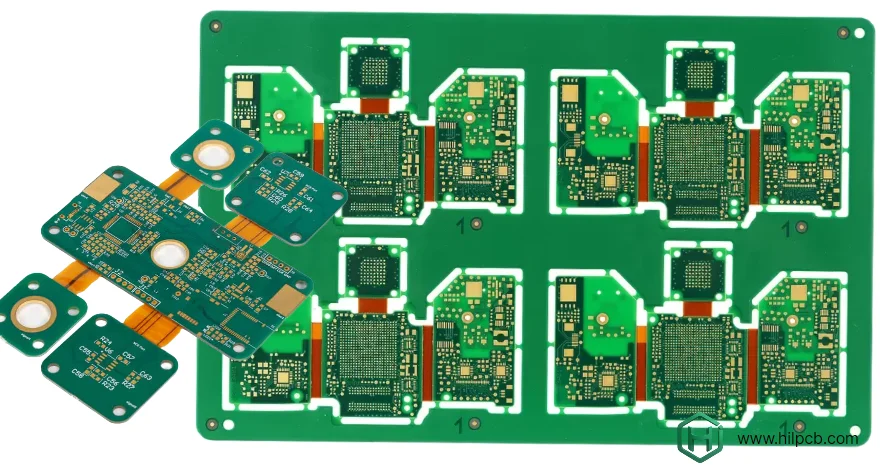
Renewable-energy inverters are becoming smaller, faster and more densely integrated. Solar inverters, wind-power converters and energy-storage PCS hardware must manage high DC bus voltage, fast switching devices, accurate sensing, grid-support control and long outdoor service life. In that environment, a PCB is no longer just a carrier for components. It becomes part of the power stage, part of the insulation system, part of the thermal path and part of the electromagnetic design.
A rigid-flex PCB can be attractive in this category because it combines rigid component islands with flexible interconnect sections. Used well, it can reduce wire harnesses, eliminate some board-to-board connectors, improve packaging density and keep control signals closer to the power stage. Used poorly, it can also create new risks: bend fatigue, insulation uncertainty, copper-thickness imbalance, material transition stress and inspection difficulty.
This guide explains how to review a rigid-flex PCB for renewable-energy inverter hardware. It focuses on board-level design and manufacturing decisions, not on claiming that a PCB alone proves inverter safety, grid compliance or efficiency. For inverter certification, the complete product still needs system-level design review, environmental testing, insulation verification, EMC testing and grid-code validation.
Key takeaways
- Rigid-flex is most useful when it replaces unreliable harnessing or shortens critical signal paths, not when it is added only for novelty.
- High-voltage inverter boards need creepage, clearance, insulation coordination and contamination planning before mechanical folding is frozen.
- SiC and GaN switching make loop inductance, common-mode noise, gate-drive return paths and Kelvin-source routing more sensitive than in slower silicon designs.
- Heavy copper, copper coin, thermal via arrays and mechanical heat sinking must be planned with manufacturable stackup limits, not added late.
- The flex section is usually best for controlled interconnect and packaging freedom; high-current and high-heat functions usually belong on rigid islands.
- A rigid-flex inverter RFQ should include voltage class, current paths, bend radius, flex-cycle expectations, insulation requirements, thermal loads and assembly constraints.
In this guide
- Where rigid-flex PCBs fit in renewable-energy inverters
- High-voltage isolation, creepage and clearance
- SiC and GaN gate-drive layout
- High-current copper and thermal paths
- EMI, EMC and grid-tie noise control
- Rigid-flex stackup and manufacturability
- Assembly, inspection and validation
- Common failure modes
- Cost drivers and RFQ checklist
- FAQ
Where rigid-flex PCBs fit in renewable-energy inverters
A renewable-energy inverter normally contains several electronics zones. The high-power path handles the DC link, power modules, busbars, current sensors, protection devices and AC output filtering. The control path handles MCU, DSP or FPGA logic, isolation interfaces, gate-drive command generation, sensing, communication and diagnostics. Auxiliary boards may support fans, relays, contactors, display interfaces, wireless modules or data logging.
Rigid-flex is not automatically the right answer for every one of these zones. It is most valuable where the electrical and mechanical packaging problems overlap. For example, a rigid-flex assembly can connect a control board to a gate-driver daughter island without a cable harness. It can wrap around a mechanical heatsink or enclosure. It can route low-current signals through a controlled, repeatable path while rigid islands carry the components and thermal structures.
The important design question is not “Can this inverter use rigid-flex?” The better question is: “Which interfaces become safer, shorter, cleaner or more reliable if they are implemented as a rigid-flex structure?”
| Inverter area | Rigid-flex value | Main caution |
|---|---|---|
| Gate-driver connection | Shorter driver-to-switch paths and fewer connectors | Keep isolation, return path and dv/dt coupling under control |
| Sensing board to control board | Repeatable low-noise interconnect for voltage, current and temperature data | Protect analog signals from power-stage noise and flex stress |
| Front-panel or communications interface | Packaging freedom and reduced harnessing | Avoid routing noisy or safety-critical nets through uncontrolled bends |
| Power-stage current path | Usually better on rigid heavy-copper regions or busbars | Flex copper is not a substitute for a busbar without careful current and heating analysis |
| Thermal interface area | Rigid islands can mount to heatsinks or cold plates | Do not rely on the flex section as a primary heat spreader |
For HILPCB, the most successful rigid-flex inverter projects usually start with a mechanical and electrical partitioning review. The customer identifies what the flex section must replace, what it must not carry, where it will bend, and how the assembly will be installed. Only then does stackup design become meaningful.
High-voltage isolation, creepage and clearance
Renewable-energy inverters often operate with high DC bus voltages and significant transient stress. Utility-scale PV, energy storage and industrial power conversion systems may also face altitude, humidity, dust and pollution concerns. In this environment, insulation design must be treated as a product-level requirement that is supported by the PCB, not as a last-minute DRC rule.
Rigid-flex can help with physical separation because high-voltage and low-voltage circuits can be placed on different rigid sections. A flex link can provide a controlled interconnect path while allowing the rigid islands to sit in mechanically separate zones. This can reduce connector count and make packaging more compact. However, the flex region must still be reviewed for dielectric thickness, conductor spacing, coverlay openings, adhesive systems, bend radius and contamination exposure.
A common mistake is assuming that a flex section automatically creates safer isolation because it is physically longer. The real question is whether the completed assembly maintains the required creepage and clearance after folding, mounting, coating, potting, enclosure compression and field aging.
High-voltage review points
| Review item | What to check | Why it matters |
|---|---|---|
| Voltage class | DC bus voltage, AC output voltage, surge/transient category and expected overvoltage | Determines spacing, insulation and test strategy |
| Pollution environment | Indoor cabinet, outdoor inverter, sealed enclosure, dust, salt fog or humidity | Contamination can reduce surface insulation margins |
| Creepage path after forming | Spacing along the real folded surface, not only flat CAD view | Folding can shorten or expose practical creepage paths |
| Flex coverlay openings | Exposed copper, stiffener edges, adhesive squeeze and connector transitions | Openings can become weak insulation points |
| Slots and cutouts | Whether slots improve creepage without weakening rigid islands | Mechanical stiffness and insulation both matter |
| Hi-pot access | Repeatable test points and fixture strategy | Volume testing must be consistent and safe |
For PV and DER products, IEC 62109, UL 1741 and IEEE 1547 are system-level or equipment-level references. A PCB can support the required insulation, spacing, protection and test access, but the completed inverter still needs product-level verification.
SiC and GaN gate-drive layout
Wide-bandgap devices such as SiC MOSFETs and GaN transistors allow higher switching speeds and higher power density. They also make layout mistakes more visible. Fast voltage and current transitions can turn small parasitic inductance into overshoot, ringing, false turn-on, excessive common-mode current and EMI failures.
A rigid-flex PCB can help because it may allow the driver island to sit close to the power device while still connecting back to the main control board. Shorter gate-drive paths can reduce loop inductance and improve waveform control. The flex section can also replace a cable that would otherwise behave like an uncontrolled antenna.
The layout still needs discipline. A short gate trace is not enough if the return path is poor. The gate loop, source/Kelvin return, local decoupling, isolation barrier and protection network must be reviewed as a complete structure.
Gate-drive layout priorities
- Place the isolated driver, local bootstrap or bias supply, turn-on/turn-off resistors and Miller clamp close to the power switch or module pins.
- Keep gate and return paths paired so the loop area stays small.
- Use Kelvin source or Kelvin emitter connections where the power device or module provides them.
- Keep desaturation, short-circuit detection and soft-shutdown paths away from high dv/dt noise.
- Place local decoupling capacitors directly at the driver supply pins with a compact return path.
- Avoid routing sensitive gate-control signals across noisy switching nodes or flex bends without a stable reference.
- Confirm the flex stackup can provide the reference structure needed for the signals it carries.
| Design choice | Benefit | Risk if poorly implemented |
|---|---|---|
| Rigid island near power module | Shorter gate loop and cleaner driver placement | Thermal exposure from the power stage may reduce driver lifetime |
| Flex interconnect to controller | Fewer cables and more repeatable signal path | Bend stress or EMI coupling can affect control signals |
| Microvia or HDI escape | Compact routing around dense driver packages | Stacked microvia reliability must be qualified for thermal cycling |
| Shielded flex reference | Better noise control for sensitive nets | Added layers increase thickness, cost and bend constraints |
| Connector elimination | Higher vibration reliability and lower assembly variability | Rework becomes harder if the integrated assembly is not planned well |
For high-speed digital control lines, HILPCB can support high-speed PCB manufacturing discipline, but inverter gate-drive success depends on the customer’s circuit architecture, simulation, waveform validation and system-level EMC testing as well as board fabrication.
High-current copper and thermal paths
Rigid-flex PCBs are often discussed as a packaging technology, but inverter hardware also needs robust power and thermal design. High-current paths generate I²R losses, and power devices, drivers, shunts, relays and protection devices can create localized heating. The rigid sections usually carry the heavy electrical and thermal burden, while the flex sections provide routing freedom for lower-current interconnect.
Heavy copper PCB is useful where current density and temperature rise drive the layout. Wider copper, multiple parallel paths, stitched planes and controlled copper balance can reduce resistance and improve heat spreading. In selected rigid regions, embedded copper coin or copper inlay can create a lower thermal-resistance path from a device to a heatsink, baseplate or cold plate.
The key is to avoid treating copper thickness as a magic answer. Heavy copper affects etching capability, spacing, solder mask registration, lamination balance, minimum trace/space, panel yield and assembly thermal profile. Copper coin structures require mechanical registration, reliable bonding, flatness control and compatible assembly pressure.
Thermal and current strategy table
| Technique | Best use | Manufacturing caution |
|---|---|---|
| Heavy copper | High-current pours, power distribution, heat spreading | Fine-pitch routing becomes harder as copper weight increases |
| Parallel copper layers | Distribute current and reduce temperature rise | Via current sharing and layer transitions must be designed, not assumed |
| Thermal via arrays | Move heat from component pads to internal or backside copper | Via fill, solder wicking and assembly plan must be controlled |
| Copper coin / copper inlay | Local high-heat devices, power modules or high-flux components | Plan flatness, bonding, solderability and mechanical tolerance early |
| Metal stiffeners or heatsink interface | Improve mechanical support and heat transfer | Verify insulation and thermal interface pressure |
| Rigid-flex partitioning | Keep hot power areas on rigid islands and route controls through flex | Flex sections should not be overloaded thermally or mechanically |
For inverter power hardware, thermal validation should use production-like enclosures, heatsinks, airflow, potting or coating conditions. A bare-board thermal simulation does not capture every field condition.
EMI, EMC and grid-tie noise control
Inverters are electrically noisy products. Switching transitions, common-mode current paths, long cable connections, magnetics, relays and enclosure geometry all affect conducted and radiated emissions. Rigid-flex can reduce some noise paths by removing cables and shrinking loops, but it can also introduce new coupling routes if the flex is used carelessly.
Grid-tie products must ultimately be evaluated at the equipment level. IEEE 1547 addresses DER interconnection and interoperability requirements, while UL 1741 and IEC 62109 are commonly used in product safety and certification workflows. The PCB contributes to these outcomes by controlling loop area, isolation, grounding, filter placement, surge paths and connector interfaces.
EMI-aware rigid-flex practices
- Keep high dv/dt switch nodes compact and away from flex regions unless the return and shielding structure is deliberate.
- Route isolated feedback, current sensing and temperature sensing away from common-mode noise sources.
- Put common-mode chokes, Y-capacitors, surge protectors and filter components where their return paths are short and controlled.
- Avoid creating long flex loops that can radiate or receive noise.
- Use stitching vias and reference planes around noisy rigid sections where stackup allows.
- Plan shield terminations and chassis connections with the mechanical enclosure team.
- Keep communication interfaces such as CAN, RS-485, Ethernet or wireless modules away from high-current switching loops.
| Noise source | Board-level countermeasure | Validation needed |
|---|---|---|
| Gate-drive ringing | Short loop, proper return, damping resistor options, Kelvin source routing | Double-pulse test and waveform review |
| Common-mode current | Compact switching node, controlled Y-cap path, shielding and chassis strategy | Conducted/radiated EMC pre-scan and final system test |
| Sensor pickup | Separate analog front end, filtering, guarding and stable reference | Accuracy test under switching load |
| Communication errors | Isolation, TVS/ESD protection and differential routing discipline | Protocol test under surge/EFT/EMI stress |
| Flex antenna effect | Short flex length, paired returns, shielding if needed | Radiated emissions and immunity testing |
Rigid-flex stackup and manufacturability
Rigid-flex manufacturing is less forgiving than standard rigid PCB fabrication. The design combines different material systems, different copper thicknesses, different mechanical behavior and different assembly constraints. For renewable-energy inverters, the challenge increases because the product may also demand high voltage spacing, heavy copper, conformal coating, selective soldering, high-current terminals and long-term thermal cycling.
A manufacturable stackup starts by separating what each region must do. The rigid power island may need high copper weight, robust through-hole plating and heatsink mounting. The control island may need fine-pitch SMT, HDI escape, impedance control and dense test access. The flex section may need controlled bend radius, limited layer count, rolled annealed copper, coverlay, stiffeners and strain relief.
Trying to force all regions into one “maximum performance” stackup can create unnecessary cost and yield risk. A good rigid-flex design is selective: power where power is needed, fine routing where fine routing is needed, and bend reliability where bending is unavoidable.
Stackup decisions to freeze early
| Decision | Why it matters |
|---|---|
| Static bend vs dynamic bend | Dynamic flex cycles require more conservative copper, bend radius and construction choices |
| Bend radius and bend direction | Copper grain direction, layer count and adhesive structure affect fatigue risk |
| Flex layer count | More flex layers improve routing but reduce flexibility and raise stress |
| Copper type in flex | Rolled annealed copper is often preferred for flexing, while electrodeposited copper may be used in less dynamic areas |
| Rigid copper weight | Heavy copper improves current handling but limits fine features and increases etch compensation needs |
| Stiffener locations | Stiffeners protect components and connectors but can create stress concentration at transitions |
| Surface finish | ENIG, ENEPIG, immersion silver or OSP should match soldering, bonding, shelf-life and cost needs |
| Coating or potting | Protective materials can change creepage behavior, thermal transfer, reworkability and inspection access |
HILPCB’s rigid-flex PCB review typically starts with bend drawings, stackup targets, voltage spacing rules and assembly constraints, because those details determine whether the board can be built repeatably.
Assembly, inspection and validation
A renewable-energy inverter rigid-flex PCB must survive more than fabrication. It must also survive assembly handling, forming, cleaning, coating, potting, functional testing, installation and field operation. This is where early PCBA planning matters.
Assembly fixtures should support the board during SMT, reflow, selective soldering, press-fit insertion or screw-terminal installation. Flex sections need protection from accidental creasing. Heavy components on rigid islands need support so that vibration does not transfer stress into the flex transition. Conformal coating and potting should be evaluated for coverage, bubbles, cure shrinkage, reworkability and interaction with high-voltage spacing.
Recommended validation flow
- DFM/DFx review: Check stackup, bend radius, copper balance, creepage/clearance, panelization, test access and assembly fixtures.
- Bare-board electrical test: Verify continuity, isolation, controlled nets and coupons where applicable.
- Incoming and in-process inspection: Use AOI, dimensional checks and cross-section sampling for critical builds.
- SMT and THT assembly control: Validate solder paste, reflow profile, selective soldering, terminal solder quality and cleaning.
- Forming and mechanical fit check: Confirm the actual folded shape does not violate spacing, stress or enclosure assumptions.
- Hi-pot and insulation test: Execute project-defined high-voltage verification with repeatable fixtures.
- Functional power test: Check gate-drive waveforms, bias rails, sensing accuracy, communication and protection response.
- Thermal test: Measure temperatures under realistic load, airflow, heatsink and enclosure conditions.
- EMC pre-scan: Identify layout-driven emissions or immunity issues before full certification testing.
- Reliability stress: Apply thermal cycling, vibration, humidity or power cycling according to the product use case.
Common failure modes
| Failure mode | Likely cause | Prevention strategy |
|---|---|---|
| Cracked copper in flex bend | Bend radius too tight, wrong copper type, dynamic flexing not declared | Define static/dynamic bend, use appropriate flex construction and add strain relief |
| Delamination at rigid-flex transition | Material mismatch, poor stress relief, thermal cycling | Use proper transition design, stiffeners and qualified lamination process |
| Insulation breakdown | Inadequate spacing, contamination, coating voids, folded geometry not reviewed | Verify creepage/clearance after forming and plan cleaning/coating controls |
| Gate-drive ringing | Long loop, poor return path, parasitic inductance, weak decoupling | Shorten driver loop, use Kelvin return and validate with switching tests |
| Sensor drift or false trips | Common-mode noise, poor analog grounding, inadequate filtering | Separate sensing from power noise and test under real switching conditions |
| Hot terminals or copper paths | Underestimated current density, poor via sharing, solder joint heating | Use current calculations, thermal test and heavy-copper or busbar strategy where justified |
| Coating-related leakage | Residue under coating, bubbles, edge coverage gaps | Clean before coating and verify coverage around high-voltage areas |
| Rework damage | Integrated rigid-flex structure not designed for repair | Define rework limits and avoid placing fragile flex near high-rework components |
Cost drivers and RFQ checklist
Rigid-flex inverter boards can reduce system assembly complexity, but the board itself is usually more expensive than a simple rigid PCB. Cost is driven by layer count, flex construction, material choices, copper weight, HDI features, controlled impedance, bend requirements, stiffeners, surface finish, coating, test fixtures and reliability validation.
The fastest way to control cost is not to remove all advanced features. It is to put advanced features only where they solve a real problem.
Main cost drivers
| Cost driver | Why it increases cost | How to control it |
|---|---|---|
| More flex layers | Higher lamination complexity and lower flexibility | Keep flex routing simple where possible |
| Heavy copper | Etching and registration become harder | Use heavy copper only in power regions |
| Microvia / stacked via | Higher drilling, plating and reliability qualification burden | Use only where dense packages require it |
| Copper coin or inlay | Adds mechanical and thermal-process complexity | Reserve for verified hotspots |
| Tight spacing at high voltage | Requires more review and inspection discipline | Freeze voltage rules and mechanical geometry early |
| Dynamic bend requirement | Requires more conservative flex construction | Declare whether the bend is static or repeatedly flexed |
| Coating/potting | Adds process, inspection and rework constraints | Define required protection class and keep-out areas early |
| High-voltage test fixtures | Requires custom fixture and safety process | Include test method in the RFQ package |
RFQ checklist for rigid-flex inverter PCBs
Send the following with your RFQ to reduce back-and-forth and avoid inaccurate pricing:
- Gerber, ODB++, IPC-2581 or native CAD export
- Schematic or at least net-class information for high-voltage, high-current and sensitive signals
- Preliminary stackup or required layer count
- DC bus voltage, working voltage, transient voltage and insulation requirements
- Creepage and clearance rules by net class
- Current requirements for power paths, terminals and connectors
- Copper weight expectations by region
- Bend drawing with radius, bend direction and static/dynamic flex requirement
- Rigid island thickness, flex thickness and stiffener requirements
- Thermal requirements, hotspots and heatsink interface drawings
- Surface finish preference such as ENIG, ENEPIG, immersion silver or OSP
- Coating, potting, cleaning or no-clean requirements
- Assembly BOM, pick-and-place file and centroid data if PCBA is required
- Test requirements: electrical test, hi-pot, functional test, programming, burn-in or thermal cycling
- Expected prototype quantity, pilot quantity and annual volume
- Target certifications or equipment-level standards that the board must support
Reference standards and design evidence boundaries
Rigid-flex inverter PCBs often support equipment that is evaluated against several standards. These standards should be treated as system and product references, not as proof that a bare PCB is compliant.
- IEC 62109-1: Safety of power converters for use in photovoltaic power systems. A PCB can support insulation, layout and manufacturing evidence, but the full power converter is evaluated at equipment level.
- UL 1741: Inverters, converters, controllers and interconnection system equipment for use with distributed energy resources. PCB layout, spacing and test access support the product evaluation, but UL 1741 applies to equipment.
- IEEE 1547-2018: Interconnection and interoperability requirements for distributed energy resources. The PCB may support control, sensing and communication hardware needed by the inverter, but grid interconnection compliance is system-level.
- IEC 61800-5-1: Safety requirements for adjustable speed electrical power drive systems. This can be relevant to motor-drive and converter hardware, but the PCB alone is not the certified drive system.
- IPC-2223 / IPC-6013: Common references for flexible and rigid-flex printed board design and qualification. Project-specific acceptance criteria should still be agreed before build.
- IPC-A-610 / J-STD-001: Assembly workmanship and soldering references for PCBA acceptance. They do not replace inverter-level safety or EMC validation.
Why work with HILPCB on inverter rigid-flex PCBs?
HILPCB supports rigid-flex PCB fabrication and PCBA assembly for power electronics projects that need packaging density, high-voltage spacing, controlled manufacturing and repeatable test planning. For renewable-energy inverter teams, the most valuable support usually happens before the first prototype: stackup review, bend-risk review, copper strategy, DFM, test-point planning and assembly-process alignment.
Useful HILPCB routes for this kind of project include rigid-flex PCB, heavy copper PCB, high-Tg PCB, SMT assembly, through-hole assembly and turnkey assembly.
For a quote, prepare the RFQ checklist above and upload the package through the Quote page. If the board includes high voltage, high current or dynamic flexing, include those constraints in the first message so the engineering review starts with the real risk drivers.
FAQ
Why are rigid-flex PCBs useful in renewable-energy inverters?
Rigid-flex PCBs can reduce connectors and wire harnesses, improve packaging density and make some gate-drive or sensing paths more repeatable. They are especially useful when the inverter has multiple rigid electronics zones that must be connected through a compact mechanical structure.
Can a rigid-flex PCB carry inverter power current?
It can support current paths when designed correctly, but the rigid sections usually handle the heavier current using wide copper, parallel layers, heavy copper, busbar interfaces or copper inlays. The flex section should not be treated as a high-current bus unless current density, heating, bend stress and insulation have been carefully validated.
Does rigid-flex automatically improve high-voltage isolation?
No. Rigid-flex can help physical partitioning, but creepage, clearance, coverlay openings, adhesive systems, folded geometry, coating and contamination exposure still need formal review. Isolation must be checked on the final formed assembly, not only in the flat layout.
What is the main risk with SiC or GaN inverter rigid-flex designs?
Fast switching makes parasitic inductance, return paths and common-mode coupling more critical. The gate-drive loop, local decoupling, sensing references and flex shielding need to be planned together and then validated with real switching waveforms.
What should be frozen before prototyping?
Freeze voltage class, bend radius, static or dynamic flex requirement, copper weight, stackup, rigid island thickness, creepage and clearance rules, thermal interface assumptions, coating or potting requirements and test access. Changing these after the first build can force a complete redesign.
Can HILPCB build and assemble rigid-flex inverter PCBs?
HILPCB can support rigid-flex fabrication, heavy-copper regions, SMT assembly, through-hole assembly and turnkey PCBA workflows depending on the project requirements. The manufacturability review should start with full design files and clear voltage, current, bend and thermal constraints.