

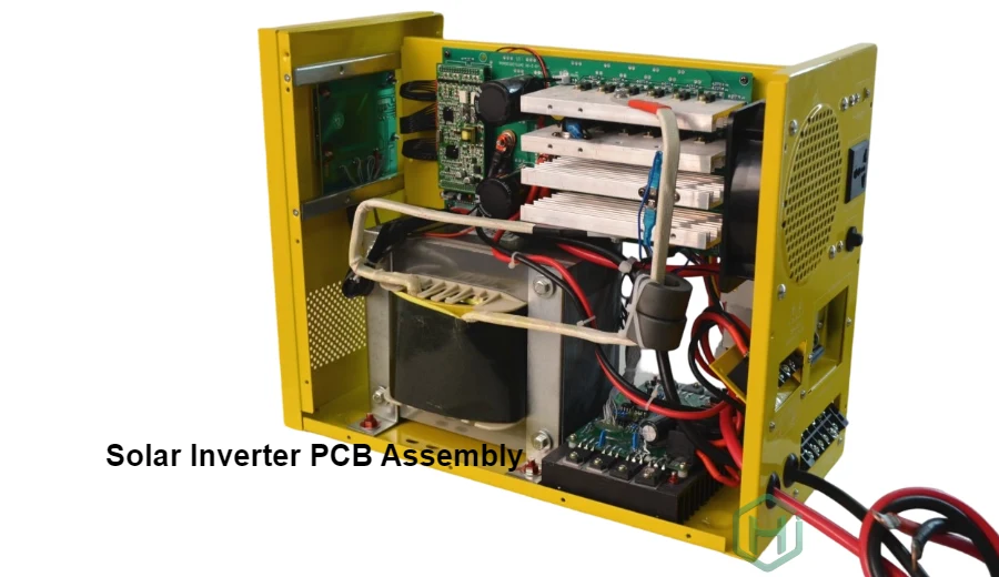
Solar power deployments continue to grow worldwide, and inverter reliability has become a defining factor for system uptime and lifecycle cost. Inside every inverter, the PCB must survive high voltage stress, sustained current loading, temperature cycling, moisture exposure, and strict EMC constraints—often for a 20–25 year service life.
This guide explains how to engineer and manufacture solar inverter PCBs that meet real-world power-electronics requirements, from material selection and stackup planning to process controls and long-term quality standards.
1. Understanding Solar Inverter Types and Their PCB Requirements
Solar inverters come in multiple architectures, and each form factor creates a different “failure profile” for the PCB. Compact inverters struggle with heat density and environmental sealing, while large inverters demand robust power distribution and insulation margins.
At HILPCB, we align board design, materials, and process controls to the inverter’s thermal envelope, current profile, and compliance target—so certification and reliability are built in from the start.
Key PCB Requirements by Inverter Type
- String inverters (residential/commercial): High DC input voltage, strong isolation between power/control zones, stable thermal behavior under continuous load.
- Microinverters (module-level): Ultra-compact footprints, wide temperature range operation (-40°C to +85°C), humidity resistance, high power density per cm².
- Central inverters (utility scale): High current capability, mechanically stable boards, scalable manufacturability, and industrial-grade reliability for long duty cycles.
Choosing the right stackup and process window early prevents late-stage redesigns, reduces qualification risk, and improves yield when scaling from prototype to volume.

2. Managing Voltage Isolation, Current Capacity, and Thermal Stress
Solar inverter PCBs face conditions that typical commercial electronics rarely encounter: higher voltages, larger temperature gradients, and continuous high-power switching. Small layout mistakes can trigger partial discharge, insulation breakdown, hot spots, or EMC non-compliance.
At HILPCB, our engineering team treats inverter boards as a system-level challenge—balancing creepage/clearance, power integrity, and thermal stability in one coordinated design rule set.
Key High-Power PCB Design Techniques
- Creepage & clearance engineering: Clearance spacing, slot isolation, and keep-out zones are planned around certification requirements and pollution degree, not just layout convenience.
- High-current copper strategy: For power stages and DC bus regions, heavy copper PCBs are used to reduce resistive loss, lower temperature rise, and improve current stability.
- Low-impedance power distribution: Controlled return paths, short loop areas, and segmentation rules reduce switching noise and make EMI filtering more effective.
- Thermal via networks: Dense via arrays under MOSFETs/IGBTs and rectifiers conduct heat to inner planes or heatsinks, helping maintain junction temperature margins.
- Material + stackup thermal tuning: Where insulation and heat transfer must coexist, selective use of high-thermal PCBs improves heat spreading without sacrificing dielectric performance.
- Placement-driven thermal balance: Heat sources are distributed to avoid clustered hot zones and to match airflow and heatsink contact geometry.
When these design controls are applied early, inverter boards maintain stable efficiency, reduce component stress, and pass safety/EMC testing with fewer iterations.
3. Selecting Materials That Survive Long Duty Cycles
Material choice directly impacts solder-joint reliability, insulation stability, and long-term warp/delamination behavior. In solar inverters, “good enough” FR-4 often fails sooner due to continuous heat and repeated thermal cycling.
At HILPCB, we recommend laminate systems based on real operating temperature, assembly profile (lead-free), and lifecycle expectations—not only on BOM cost.
Key Material Selection Guidelines
- Control and low-power sections: Standard FR4 PCBs are often sufficient where temperatures and current are moderate, and insulation stress is lower.
- High-power and lead-free assemblies: high-Tg PCBs provide better thermal stability, helping reduce delamination risk and improving reliability under sustained heat.
- Copper foil selection: Heavy copper starting weights, low-profile copper for certain interfaces, and adhesion-optimized foils are selected based on layer count and current density.
- Surface finish planning: ENIG, immersion silver, OSP, or hard gold are chosen based on pitch, shelf-life expectations, and contact-cycle needs.
A material system that matches the inverter’s real operating environment reduces field failures and improves warranty performance over multi-decade lifetimes.
4. Achieving EMC and Safety Compliance at the PCB Level
Many inverter compliance issues originate in PCB return paths, switching loops, and segmentation decisions. EMC filters can only do so much if the layout itself creates large loop areas or noisy coupling into control circuitry.
At HILPCB, we design for compliance by controlling current return paths, grounding strategy, and noise containment before the first prototype build.
Key EMC & Safety Implementation Practices
- Ground integrity: Continuous reference planes and predictable return paths minimize high-frequency radiation and improve signal stability.
- Noisy vs. sensitive partitioning: Switching nodes and gate-drive regions are physically isolated from sensing, analog control, and communication sections. This also protects DC-side sensing for solar arc fault detection.
- Filtering and shielding readiness: Footprints and mounting features for filters and shields are integrated early to avoid rework in later compliance testing.
- Isolation verification readiness: Test points and isolation structures support production-level verification and documentation for certification.
Designing for compliance from day one reduces re-spin cycles and accelerates time-to-certification.

5. Controlling Manufacturing Variables for High-Reliability Output
Even a strong design can fail in the field if manufacturing controls are not tuned for heavy copper, multilayer registration, and high-aspect-ratio vias. Solar inverter PCBs demand stable process windows and traceable documentation.
At HILPCB, we combine process capability control with DFM reviews for solar inverter PCBs to keep yield high and quality consistent—especially when moving from proto to volume.
Key Manufacturing Process Controls
- Heavy copper fabrication control: Imaging, etching compensation, plating uniformity, and press cycles are adjusted for thick copper topography and via reliability.
- Stackup and registration accuracy: For complex power/control designs, multilayer PCBs require strict dielectric thickness control, copper balance, and registration stability to prevent warpage and impedance drift.
- Electrical verification: Beyond continuity tests, hi-pot testing, impedance verification (when needed), and thermal screening help detect risks before assembly.
For OEMs and EMS partners, strong process control translates into fewer line stoppages, fewer escapes, and better long-term field stability.
6. Building to Quality Standards That Match a 20–25 Year Lifetime
Solar inverters are expected to run continuously with minimal maintenance. PCB quality standards must therefore address long-term mechanisms like via fatigue, solder joint cracking, and moisture-driven leakage.
At HILPCB, we align inspection criteria, reliability testing options, and traceability records with the service life expectations of photovoltaic power electronics.
Key Quality and Reliability Practices
- Standards alignment: IPC-6012, IPC-A-600 (Class 2/3), IPC-A-610, ISO 9001, and—where applicable—automotive-grade requirements.
- Reliability testing options: Thermal cycling, 85°C/85% RH humidity exposure, vibration simulation, and accelerated stress testing can be used for design validation.
- Full traceability: Material lots, process parameters, and test records are retained for warranty support and continuous improvement.
Reliable documentation and disciplined quality control reduce long-tail failure risk and support global compliance requirements.
7. Scaling from Prototype to Volume Without Losing Consistency
Scaling inverter production is not only a capacity challenge—it’s a consistency challenge. Minor variations in materials, plating thickness, or press conditions can shift thermal behavior and reliability.
At HILPCB, we support ramp-up by keeping process windows stable, controlling supplier qualification, and delivering engineering feedback before issues appear at assembly.
Key Partner Capabilities to Evaluate
- Proven experience with high-voltage isolation and high-current layouts
- Heavy copper and multilayer process maturity
- In-house electrical test capability and documentation discipline
- DFM + stackup support to reduce revision cycles
If you also require assembly and component sourcing coordination, turnkey assembly can simplify your supply chain and shorten the path from prototype builds to production ramp.
8. Optimizing Cost Without Compromising Reliability
Solar inverter boards require premium materials and controlled processes, but cost can still be optimized through engineering choices that protect yield and reduce rework.
Practical Cost Optimization Methods
- Panelization efficiency: Improve utilization within standard panel sizes to reduce cost per board.
- Right-fit materials: Use higher-grade laminates only where thermal and lifecycle requirements demand it.
- DFM-first layout: Avoid unnecessary tight tolerances that increase scrap or reduce throughput.
- Volume planning: Consolidate recurring orders to stabilize lead time and pricing.
Cost optimization works best when it supports yield, reliability, and certification—not when it undercuts them.
Conclusion
Solar inverter PCB manufacturing combines high-power electrical design, harsh-environment reliability, and strict compliance requirements. Success depends on getting fundamentals right: isolation structures, current and thermal design, stable materials, and disciplined manufacturing controls.
For inverter OEMs and power-electronics teams, choosing a manufacturer with proven high-power process capability and engineering support is one of the most effective ways to reduce qualification risk and deliver long-life products at scale.