
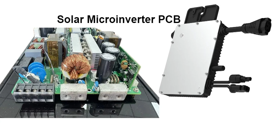
A solar microinverter PCB operates in one of the harshest environments in power electronics. Installed directly behind photovoltaic modules, it must perform continuous DC–AC conversion inside a compact, sealed enclosure while exposed to heat, moisture, vibration, and long-term outdoor aging.
In many microinverter products, performance limitations and early failures are not caused by control algorithms, but by PCB-level constraints. Power density, thermal dissipation, isolation spacing, and manufacturing consistency all directly influence efficiency, reliability, and service life.
This guide explains how solar microinverter PCB design and manufacturing decisions affect real-world performance, focusing on layout strategy, thermal control, material selection, and production readiness.
Managing Power Density in Solar Microinverter PCB Design
Solar microinverters integrate power conversion, control, protection, and communication functions into a very limited PCB area. As output power increases, current density rises sharply, leaving little margin for inefficient routing or excessive parasitics.
Poor power distribution at the PCB level often leads to higher losses, EMI issues, and localized overheating.
Key Power Density Design Techniques
- Short, wide current paths: High-current traces and pours are designed to minimize resistive loss.
- Layer-based power routing: Well-structured multilayer PCBs provide low-impedance return paths and support compact layouts.
- Switching loop minimization: Input and output power loops are tightly coupled to reduce parasitic inductance.
- Component clustering: Power switches, drivers, and decoupling capacitors are placed to minimize loop area.
- Enhanced copper thickness: For higher-power designs, heavy copper PCBs improve current handling and thermal stability.
Effective power density management is the foundation of reliable solar microinverter PCB performance.
Thermal Management for Outdoor Solar Microinverter PCBs
Solar microinverters typically rely on passive cooling. Heat generated by power devices must travel through the PCB and enclosure before being dissipated to ambient air.
Thermal bottlenecks at the PCB level are a common cause of reduced lifetime and field failures.
Key Thermal Management Techniques
- Copper heat spreading: Large copper pours and internal planes distribute heat away from localized hotspots.
- Thermal via arrays: Dense vias beneath MOSFETs and rectifiers transfer heat into inner layers or the opposite PCB side.
- High-temperature laminate stability: high-Tg PCBs reduce delamination risk under thermal cycling and lead-free reflow.
- Enhanced thermal substrates: In compact, high-power sections, high-thermal PCBs improve heat dissipation without sacrificing insulation.
- PCB-to-housing interface: Flat contact zones and thermal interface materials support efficient heat transfer to the enclosure.
A well-designed thermal path is essential for maintaining long-term reliability in outdoor solar microinverter PCBs.
Signal Integrity and EMI Control in Solar Microinverter PCBs
Modern solar microinverters operate at higher switching frequencies to improve efficiency and reduce magnetic size. This increases sensitivity to layout-induced noise and electromagnetic interference.
EMI challenges are often resolved—or created—at the PCB level.
Key EMI-Oriented Layout Practices
- Continuous reference planes: Solid ground planes provide predictable return paths for high-frequency currents.
- Functional zoning: Power switching areas are physically separated from control and communication circuits.
- Controlled routing: Sensitive signals avoid high dv/dt nodes and fast gate-drive paths.
- Impedance-aware interfaces: For monitoring and communication signals, high-speed PCBs help maintain signal integrity.
- Filtering at entry points: External interfaces include appropriate filtering and surge protection.
EMI-aware PCB design reduces certification risk and improves production consistency.
Material Selection for Long-Life Solar Microinverter PCBs
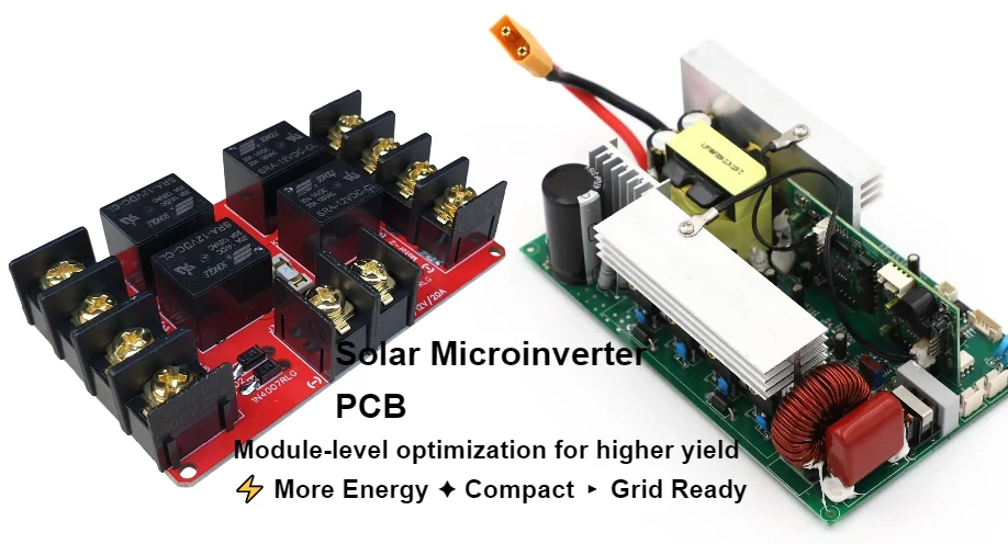
Outdoor solar microinverter PCBs must operate reliably for decades. Temperature cycling, moisture exposure, and mechanical stress place continuous demands on PCB materials and interconnects.
Material choices directly influence lifetime and stability.
Key Reliability-Focused Material Decisions
- Base laminate: High-Tg FR-4 systems with stable thermal and mechanical properties.
- Surface finish: Corrosion-resistant finishes compatible with conformal coating.
- Mechanical balance: Symmetric stack-ups reduce warpage during assembly and field operation.
- Flexible interconnects: In compact layouts, flex PCBs can support mechanical integration and vibration tolerance.
Reliability-oriented material selection reduces long-term failure risk in solar microinverter PCB applications.
PCB Architecture and System Integration Considerations
As solar microinverter designs evolve toward higher power density and increased functionality, it is increasingly common to integrate power conversion, digital control, sensing, protection, and communication circuits onto a single PCB or tightly coupled PCB assembly. Early architectural decisions at this stage directly affect electrical performance, thermal behavior, manufacturability, and long-term scalability.
A well-planned PCB architecture establishes a clear framework for layout, materials, and process selection, reducing redesign risk as products move from prototype to volume production.
Key PCB Architecture and Integration Considerations
- Functional zoning and isolation strategy: Power stages (DC-DC, DC-AC, gate drivers), low-voltage control logic, sensing circuits, and communication interfaces must be physically and electrically partitioned. Proper zoning minimizes noise coupling, simplifies EMI control, and improves system stability under high switching currents.
- Grounding and reference plane architecture: A deliberate grounding strategy—often combining solid power grounds, quiet signal grounds, and controlled return paths—is essential for accurate sensing, stable control loops, and EMI compliance.
- Optimized PCB stack-up definition: Layer count, plane placement, and dielectric thickness are selected to balance isolation voltage, controlled impedance, and thermal performance. Stack-ups must support both high-current power paths and noise-sensitive control signals without unnecessary cost escalation.
- Thermal-aware component placement: Heat-generating components such as MOSFETs, IGBTs, inductors, and rectifiers are positioned to enable efficient heat spreading through copper planes, thermal vias, and mechanical interfaces with the enclosure or heatsink.
- Connector and interface planning: DC input, AC output, communication, and sensing connectors are placed with consideration for creepage and clearance, cable routing, mechanical stress, and long-term reliability in outdoor environments.
- System-level scalability: The architecture should allow future power upgrades, interface changes, or regional variants without a complete PCB redesign, supporting product family expansion.
A disciplined PCB architecture simplifies layout iterations, improves electrical robustness, and provides a stable foundation for scalable manufacturing.
Manufacturing and Assembly Considerations for Solar Microinverter PCBs
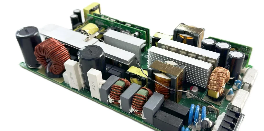
Solar microinverter PCBs are produced in high volumes and expected to operate reliably for many years in harsh outdoor conditions. Manufacturing and assembly quality therefore play a decisive role in product lifetime, safety, and warranty cost.
Designs that account for real fabrication and assembly constraints achieve higher yields, more consistent performance, and smoother transitions from prototype to mass production.
Manufacturing-Oriented PCB Design Practices
- Controlled copper distribution and current paths: Even copper balance across layers reduces warpage, improves lamination stability, and supports consistent soldering. High-current paths are reinforced using wider traces, copper pours, parallel layers, or heavy copper where required.
- Mixed-technology assembly support: Solar microinverter PCBs typically combine fine-pitch SMT control circuitry with large, high-current components assembled via through-hole assembly. Pad design, hole sizing, and soldering methods must support both technologies reliably.
- Soldering and thermal process compatibility: Pad geometry, solder mask openings, and component spacing are designed to support stable reflow and selective soldering, avoiding voids, tombstoning, or insufficient fillets on power components.
- Protective coatings and environmental resistance: PCB designs account for conformal coating or potting requirements by controlling keep-out areas, coating thickness, and component spacing to ensure long-term protection against moisture, dust, and temperature cycling.
- Test and inspection accessibility: Layouts include dedicated test points, probing access, and clear functional boundaries to support AOI, in-circuit testing (ICT), functional testing, and hi-pot verification without excessive manual intervention.
- Process repeatability and documentation: Stable manufacturing depends on consistent stack-ups, clearly defined tolerances, and traceable process parameters aligned with IPC standards.
Manufacturing-aware PCB design directly improves first-pass yield, reduces rework, and shortens the path from engineering validation to stable volume production.
Conclusion
Solar microinverter PCBs operate at the intersection of high power density, thermal stress, EMI control, and long-term outdoor reliability. Meeting these demands requires more than correct schematics—it depends on disciplined PCB architecture, material selection aligned with electrical and thermal requirements, and manufacturing processes that remain stable at scale.
HILPCB supports solar microinverter PCB fabrication and assembly with proven experience in power electronics and industrial applications. By integrating PCB manufacturing and PCBA under a controlled, engineering-driven workflow, we help customers reduce risk, improve consistency, and maintain quality from prototype builds through long-term mass production.
For solar microinverter projects where safety, reliability, and service life are critical, working with an experienced PCB manufacturing and assembly partner ensures confidence across the entire product lifecycle.