
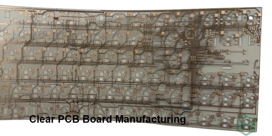
A clear PCB board is not simply a transparent version of a standard PCB. It is a product-facing circuit where appearance, optical clarity, and reliability are all critical. Many clear PCB projects look good at the prototype stage but encounter issues during scale-up, such as cosmetic defects, haze after assembly, or warpage during processing.
HILPCB is a full-service PCB manufacturing and PCB assembly factory, capable of producing all major PCB types, including clear PCB boards. By integrating fabrication and assembly under controlled processes, we help customers move clear PCB designs from prototype to stable, repeatable production.
What Makes a Clear PCB Board “Production-Ready” (Not Just “Clear”)
Clear PCB programs succeed when procurement and engineering align on one reality: transparency is not a material feature—it’s a quality system requirement.
A production-ready clear PCB board typically has:
- A visual specification (what defects are acceptable, where the viewing window is, what “clean” means)
- A process plan (handling, cleaning, reflow profile, inspection method)
- A scalability path (pilot → small batch → volume, with stable acceptance criteria)
Key “Quote-Ready” Inputs Buyers Should Provide
- Viewing zones: which areas must remain optically clean, and which can host routing/components
- Optical criteria: haze limit, scratch/particle limits, and how appearance is inspected
- Thermal constraints: maximum assembly temperature and any enclosure heat path assumptions
- Electrical class: signal speed, power density, ESD exposure, and reliability target
- Assembly scope: PCB only, PCBA, or one-stop build (including test and packaging)
A clear PCB quote becomes predictable only when the “visual” requirement is written like an engineering requirement.
Hidden Cost Drivers in Clear PCB Board Manufacturing
Many clear PCB boards become expensive for reasons that don’t show up in the BOM. The biggest cost driver is usually cosmetic yield—because defects that would be ignored on opaque boards become unacceptable on transparent ones.
Common Hidden Cost Drivers
- Handling damage: micro-scratches, edge chips, pressure marks from fixtures
- Residue and haze: flux residue, cleaning marks, or adhesive haze that appears under light
- Warp and flatness: subtle deformation that becomes obvious when installed behind optics
- Density artifacts: uneven copper density that creates visible “shadows” or patterning
- Inspection overhead: optical inspection time and tighter reject criteria
If you want stable pricing, you need stable acceptance criteria—especially for appearance.
Clear PCB Board for Keyboard PCBs: From Visual Spec to Mass Production
Transparent keyboards are a high-visibility market where the PCB is no longer a hidden part—it’s a design element. In a keyboard PCB, the user can often see the board through clear housings, key switches, and under RGB lighting. That changes the entire manufacturing priority: the PCB must scan reliably and look intentional under real lighting.
Below is a comprehensive, production-focused framework for building clear PCB boards for keyboard PCBs—without turning the project into a cosmetic lottery.
Key Keyboard PCB Requirements That Change on Clear Boards
- Lighting reality (RGB/underglow): Copper density, mask boundaries, and silkscreen choices become visible “textures.”
- Matrix routing visibility: Row/column routing can look messy unless routing is planned as part of the design language.
- Mechanical stress: Hot-swap sockets, switch insertion, plate compression, and flex from typing can introduce cracks or solder fatigue.
- Surface cleanliness: Any residue around switch pads becomes obvious when backlit.
- Consistency across batches: Enthusiast and premium keyboard markets amplify small appearance variations.
Keyboard PCB Manufacturing Strategy for Clear Boards
- Define a visual “front side”: Decide which side faces the user and treat it like a cosmetic surface.
- Route with symmetry and rhythm: Instead of “shortest path routing,” use controlled geometry (parallel runs, consistent angles, mirrored sections).
- Control copper distribution: Even copper density reduces visible banding and lowers warpage risk.
- Plan component zoning: Keep unavoidable opaque components in non-viewing zones (edge clusters, behind bezels, or under plates).
- Specify fixture-safe edges: Add protective margins and keep-out zones to avoid clamp/fixture marks.
- Design for rework limits: Clear substrates are less forgiving; define whether rework is allowed and what “rework-safe” means.
Assembly and Reliability Controls for Keyboard PCBs
- Socket and connector anchoring: Use mechanical reinforcement strategies for repeated insertion cycles.
- Reflow profile control: Clear substrates and cosmetic standards often require tighter profile windows than standard boards.
- Cleaning and residue validation: Confirm cleaning chemistry does not introduce haze or staining over time.
- Inspection under real light: Inspect under backlight and common RGB conditions—not only under factory white light.
- Packaging that protects cosmetics: Anti-scratch separation, protective film strategy, humidity control if required.
When to Use Advanced PCB Techniques in Keyboard Clear Boards
Some keyboard PCBs include dense MCU routing, USB high-speed lines, or complex LED matrices. In those cases:
- If routing density is high and you need fine features, HDI PCBs can help maintain clean routing and stable manufacturability.
- If you have fast digital lines and want repeatable signal behavior, high-speed PCBs are often the cleaner way to control consistency than “tuning by guesswork.”
- If your assembly window is tight and you need better thermal stability through soldering and aging, high-Tg PCBs can reduce warpage and process drift.
A clear keyboard PCB becomes scalable when it is treated as a visible product surface with electrical obligations, not as an electrical board with cosmetic hopes.
Assembly Planning: How Clear PCB Boards Avoid Cosmetic Yield Collapse
Clear PCB boards usually fail at assembly, not fabrication—because assembly introduces heat, contact, residue, and mechanical stress.
Key Assembly Techniques That Protect Both Yield and Appearance
- Controlled PCBA workflow: Use stable, documented processes for placement, reflow, and post-reflow handling.
- Dedicated inspection style: Optical acceptance requires the right lighting and inspection angles.
- Process selection matters: Most clear PCB programs rely on disciplined SMT assembly with additional cleanliness and handling controls.
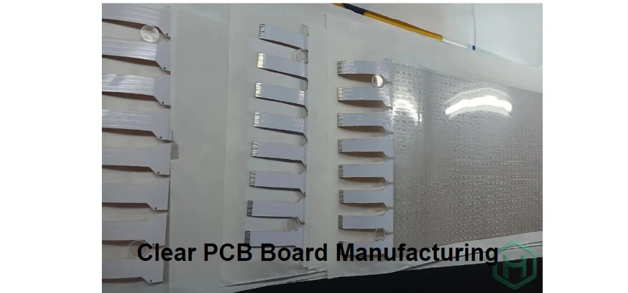
- If the product needs flexible zones: For designs combining clear windows with flex interconnects, flex PCBs can be used to move dense circuitry out of the viewing area while keeping the “window” clean.
Conclusion
A clear-pcb-board project becomes “easy” only after the hard work is done early: writing a real visual spec, defining viewing zones, choosing a manufacturable stack strategy, and locking an assembly-and-inspection workflow that protects cosmetic yield.
For teams sourcing clear PCB boards (including keyboard PCB programs), a one-stop partner can simplify responsibility boundaries and reduce coordination loss—especially when fabrication, assembly, inspection, and packaging must follow the same appearance standard. HILPCB provides PCB manufacturing and PCB assembly under a controlled workflow, including turnkey assembly options for programs that want fewer vendors, clearer accountability, and smoother scale-up.
Common Questions
What makes clear PCB boards harder to manufacture than standard FR4?
Transparent substrates reveal scratches, haze, copper show-through, and edge defects immediately, so the board has to meet cosmetic standards as well as electrical ones. The challenge is not only building the circuit, but keeping the visible surface production-safe.
How should components and traces be arranged on a clear board?
Dense circuitry, opaque components, and reinforcement features should be pushed out of the main viewing zone whenever possible. Connectors, test points, and large copper areas are usually easier to hide near edges or under covered regions.
Why do clear PCB projects need assembly and rework rules defined early?
Reflow, cleaning, fixturing, and rework can permanently change the board's appearance, so inspection lighting, acceptable defects, and rework limits should be locked before volume production. Many clear-board yield problems appear during assembly, not bare-board fabrication.