
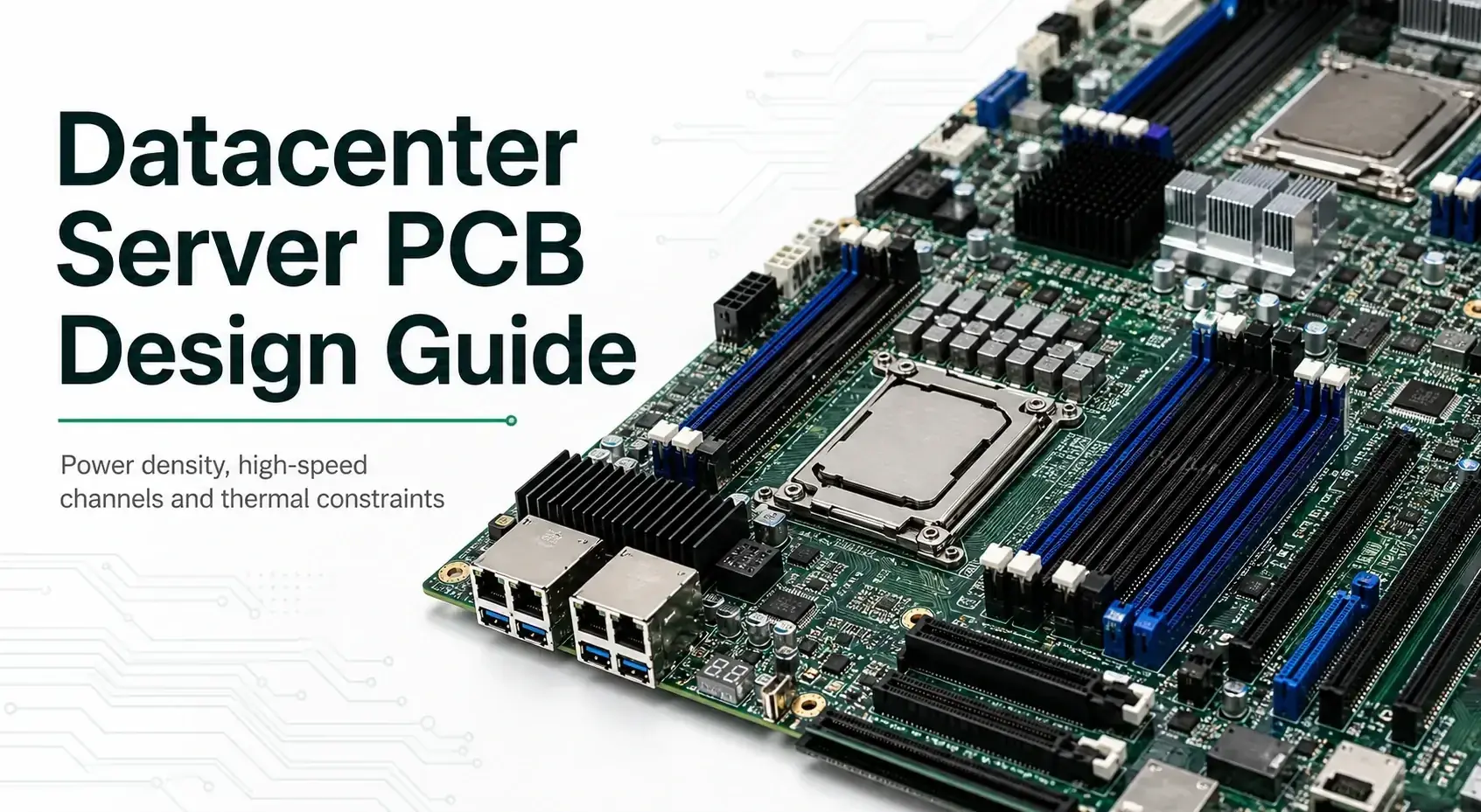
A datacenter server PCB is a high-speed, high-density board used in server motherboards, storage controllers, accelerator carriers, backplanes, switch cards, or management modules where dense interconnect, high current, strict impedance control, and staged validation determine release risk. This guide is written for hardware teams, sourcing engineers, and NPI teams that need to turn server-board intent into a manufacturable PCB package before prototype or production release.
Server terminology can easily become too broad. PCIe, DDR5, CXL, 400G, 800G, AI server, and backplane are useful context labels, but they do not prove a board is manufacturable, compliant, or validated. A strong datacenter PCB review translates those labels into board-level decisions: stackup, material loss, route class, reference continuity, connector transitions, via strategy, power delivery, thermal path, and test evidence.
Key Takeaways
- A datacenter server PCB review should start with the board type: motherboard, accelerator carrier, storage controller, backplane, riser, NIC, power board, or management module.
- Modern interface names such as
PCIe 5.0,PCIe 6.0,DDR5,400G Ethernet, and800G Ethernetcreate board-level pressure, but they do not replace simulation, coupon measurement, link validation, or system bring-up. - Stackup is not just layer count. It ties together dielectric loss, glass weave, copper roughness, impedance targets, power-plane pairing, breakout strategy, and lamination yield.
- Backdrill depth, via stub control, connector launch geometry, and return-path continuity usually matter more than nominal trace width on high-speed server boards.
- Server boards need staged validation: bare-board inspection, impedance coupon measurement, assembly inspection, power integrity checks, interface bring-up, thermal validation, and system-level correlation.
- The RFQ package should include more than Gerbers. Share stackup intent, controlled-net classes, impedance tables, drill/backdrill notes, copper weight, mechanical keepouts, connector models, and test expectations.
In This Guide
- What is a datacenter server PCB review actually deciding?
- Server board types and review routes
- How PCIe, DDR5, CXL, 400G and 800G affect PCB design
- Stackup, material and controlled-impedance planning
- SerDes routing, vias, backdrilling and connector transitions
- PDN, thermal and mechanical reliability review
- Manufacturing, inspection and validation handoff
- Common failure modes in server PCB projects
- Cost drivers and RFQ checklist
- Why work with HILPCB
- FAQ
What is a datacenter server PCB review actually deciding?
A datacenter server PCB review decides whether the board package is clear enough for manufacturing, assembly, and later system validation. It does not certify protocol compliance or guarantee link margin by itself. The practical task is to identify the board family, the interface burden, the stackup risk, the connector or backplane escalation point, and the evidence the next build must collect.
The first decision is board identity. A CPU motherboard, a GPU accelerator carrier, a storage controller, a BMC management module, a power distribution board, a riser card, and a backplane can all be described as server hardware. They should not be reviewed as the same PCB. A motherboard-style compute board is usually dominated by dense routing, memory breakout, power delivery, and thermal/mechanical constraints. A backplane is often dominated by connectors, long channels, press-fit zones, drilling precision, and large-format fabrication. A storage controller may be dominated by PCIe, SAS/SATA, NVMe, retimer placement, and connector routing. The title may say datacenter server PCB, but the design review has to be more specific.
The second decision is interface scope. Interface names explain why the board is difficult, not whether the board is already proven. PCIe 6.0 introduces PAM4 signaling and tighter channel planning than earlier PCIe generations. DDR5 changes memory power and routing expectations compared with DDR4. 400G and 800G Ethernet point toward very high-speed SerDes, optics or pluggable modules, retimers, and strict loss/crosstalk control. Those names matter, but they are still inputs to stackup and validation planning, not a substitute for proof.
The third decision is release stage. Prototype, first article, NPI, and production release should not be collapsed into one event. An early build can confirm whether the stackup, drilling, impedance coupons, connector fit, assembly process, and bring-up access are coherent. It cannot replace later eye-mask testing, BER testing, thermal chamber work, firmware bring-up, or system-level correlation.
The fourth decision is scope responsibility. A PCB manufacturer can help with stackup, DFM, impedance, material selection, lamination, drilling, backdrill, surface finish, inspection, and PCBA build controls. The final system owner must still validate server performance, protocol compliance, safety, EMI, cooling, firmware, firmware update path, and field reliability.
HILPCB can support manufacturability review, PCB fabrication, impedance-control planning, high-speed stackup review, and PCBA build coordination for datacenter hardware. Final link performance, protocol compliance, safety approvals, thermal performance, and server-level qualification must be verified at the customer device or system level.
Server board types and review routes
A useful server PCB review separates board routes before quoting. This prevents a connector-heavy board from being treated like a normal motherboard, or a high-speed riser from being quoted without the backdrill and connector-launch data that actually determine risk.
| Server hardware type | Typical board-level burden | Main PCB review focus | Related HILPCB route |
|---|---|---|---|
| Server motherboard PCB | CPU, chipset, memory, PCIe slots, management, dense power rails | Stackup, memory routing, PCIe lanes, PDN, mechanical keepouts, thermal zones | High-Speed PCB |
| Accelerator carrier PCB | GPU/AI accelerator, high-current delivery, high-speed host interface | PCIe/CXL routing, large BGA escape, copper balance, low-loss stackup, thermal vias | HDI PCB and High-Speed PCB |
| Storage controller PCB | NVMe, SAS/SATA, RAID, retimers, connectors | SerDes routing, connector launches, power sequencing, fault-tolerant design posture | High-Speed PCB |
| Backplane PCB | Multiple slots, press-fit connectors, long channels, large board size | Connector field planning, backdrill, thick board drilling, long-channel loss, inspection | Backplane PCB |
| Network interface or switch card | 25G/50G/100G+ SerDes, optics cages, retimers, hot zones | Low-loss routing, optics cage layout, power noise, thermal path, EMI boundary | High-Frequency PCB and High-Speed PCB |
| BMC or management module | Lower-speed control, security, remote management, sideband interfaces | Reliable connectors, isolation where needed, controlled production traceability | Turnkey Assembly |
| Power distribution or battery-support board | High current, hold-up energy, monitoring, safety spacing | Copper weight, thermal rise, creepage/clearance, connector current rating, DFM | Heavy Copper PCB |
| Riser card | Short but sensitive connector-to-connector paths | Edge connector geometry, impedance transition, insertion loss, mechanical tolerance | High-Speed PCB |
Not every server project needs the most expensive board route. What matters is naming the dominant burden early. A 24-layer motherboard and a connector-heavy backplane may both be difficult, but they fail for different reasons and need different manufacturing questions.
How PCIe, DDR5, CXL, 400G and 800G affect PCB design
Modern datacenter interfaces affect the board in different ways. Treat them as pressure signals, not marketing proof.
PCIe and CXL
PCIe is one of the most common high-speed interfaces on server motherboards, accelerator cards, storage controllers, and risers. Newer PCIe generations increase the pressure on loss, crosstalk, via stubs, connector transitions, return-path continuity, retimer placement, and validation planning. PCIe 6.0 moves to 64 GT/s and PAM4 signaling, while PCIe 7.0 raises the target to 128 GT/s in the official PCI-SIG roadmap and release materials. Those numbers do not mean every board should claim PCIe 6.0 or PCIe 7.0 readiness. They mean the design team must treat the channel as a measured and simulated system.
CXL uses the PCIe physical layer for cache-coherent and memory-expansion use cases. For PCB review, the practical effect is similar to PCIe: low-loss routing, consistent reference planes, clean connector transitions, and careful validation ownership. The PCB should support the physical channel; CXL protocol behavior and interoperability remain system-level matters.
DDR5 memory interfaces
DDR5 raises server-board pressure in a different way. The challenge is not a long SerDes channel to a connector. It is dense memory escape, byte-lane discipline, timing, power delivery, decoupling, and routing symmetry around DIMMs, CPUs, and sometimes memory-buffer components. DDR5 layouts are sensitive to reference continuity, via transitions, crosstalk, return-current paths, and PDN behavior.
For the fabricator, DDR5 usually translates into fine routing, stable layer registration, tight impedance process control, and clear stackup documentation. For the system owner, it still requires memory-controller bring-up, training, margining, and validation.
400G and 800G Ethernet hardware
400G and 800G server networking boards usually introduce optical cages, retimers, switch ASICs, high-speed SerDes, dense power delivery, and severe thermal hotspots. The PCB review should not promise network throughput. It should focus on the board-level items that make such hardware possible: low-loss material selection, controlled routing into cages or connectors, careful via and breakout design, clean power for SerDes/retimers, and mechanical/thermal coordination around modules.
AI server and accelerator wording
AI server PCB often means the board is carrying accelerator-adjacent pressure: large BGA packages, high-current rails, PCIe or CXL host links, dense memory or HBM-adjacent packaging at module level, high airflow or liquid-cooling constraints, and strict assembly inspection. It should not be used as a shortcut for performance claims. Translate AI server into concrete PCB burdens: layer count, copper weight, stackup loss, BGA escape, connector zones, thermal vias, power planes, and inspection plan.
| Interface or system label | What it should mean for PCB review | What it should not imply |
|---|---|---|
| PCIe 5.0 / 6.0 / 7.0 | High-speed route classification, low-loss stackup, backdrill and channel validation planning | Guaranteed compliance or link margin |
| CXL | PCIe-based physical-channel discipline plus system-level memory/coherency use case | CXL interoperability proof from PCB alone |
| DDR5 | Dense memory routing, power integrity, impedance and timing discipline | Memory training or system stability proof |
| 400G / 800G Ethernet | SerDes loss/crosstalk control, optics cage layout, retimer and thermal planning | Network throughput guarantee |
| AI server | Large package escape, high-current PDN, high-speed host links, thermal/mechanical constraints | AI performance, cluster readiness, or deployment proof |
| OCP / DC-MHS | Modular server context and mechanical/interface discipline where applicable | Automatic compatibility without system validation |
Stackup, material and controlled-impedance planning
Stackup is the foundation of a server PCB. It decides how the board balances high-speed loss, impedance targets, power-plane pairing, routing density, lamination complexity, copper balance, manufacturability, and cost.
The stackup discussion should start before layout is complete. If a server board is already routed around an unstable stackup, every later DFM fix becomes harder. Trace widths may shift, impedance may move, memory escape may need rerouting, and via transitions may no longer match the intended reference layers. On high-speed boards, stackup should be treated as a design constraint, not a fabrication afterthought.
Key stackup decisions
| Stackup decision | Why it matters | Review question before release |
|---|---|---|
| Layer count | Controls routing density, reference-plane access, power-plane pairing, and cost | Is the layer count driven by route density and reference needs, or only by legacy reuse? |
| Dielectric material | Affects insertion loss, Dk stability, Df, skew, and lamination behavior | Which layers need low-loss material, and can hybrid construction reduce cost? |
| Glass style | Can contribute to differential skew on long high-speed routes | Do long differential pairs need spread glass, routing-angle strategy, or tighter material control? |
| Copper roughness | Affects conductor loss at high frequency | Are low-profile copper options needed for critical layers? |
| Plane assignment | Determines return-current continuity and PDN behavior | Does every high-speed signal have a clean reference plane through the path? |
| Impedance targets | Translate design intent into manufacturable trace geometry | Are all controlled-net classes clearly specified with tolerances and layer references? |
| Copper weight | Drives current handling, thermal rise, and fine-line manufacturability | Are high-current layers separated from fine-pitch routing constraints? |
| Lamination cycle | Influences registration, yield, and cost | Does the design really need sequential lamination or stacked microvias? |
For very high-speed channels, avoid reducing stackup review to a single impedance number. Two boards can both target 85 Ω or 100 Ω differential impedance and still behave very differently because of dielectric loss, copper profile, via geometry, connector transitions, and fiber-weave skew.
A common server-board problem is assuming a nominal impedance value is enough. It is not. The release package should define controlled-net classes, target impedance, layer usage, width/spacing assumptions, reference planes, copper type, material family, and coupon expectations. Use an impedance calculator for planning, but treat final impedance as a stackup-and-process agreement with the fabricator.
Material selection without overclaiming
Server boards may use standard high-speed FR-4-class materials, mid-loss materials, low-loss materials, or hybrid builds. The correct choice depends on channel length, data rate, layer count, connector transitions, temperature, cost, and validation plan.
| Material route | When it may fit | Main tradeoff |
|---|---|---|
| Standard high-Tg FR-4 class | Control, management, lower-speed zones, short non-critical channels | Lowest cost, but limited loss margin for demanding high-speed paths |
| Mid-loss high-speed laminate | PCIe Gen4/Gen5-class channels where length and connector count are manageable | Better loss control with moderate cost increase |
| Low-loss laminate | Long high-speed channels, dense SerDes, retimer/optics paths, backplane-adjacent designs | Higher material and lamination cost; requires careful supplier confirmation |
| Hybrid stackup | Only selected high-speed layers require low-loss material | Cost control is possible, but lamination and Dk transition planning become more complex |
| Rigid-flex or HDI zones | Compact modules, risers, management modules, dense BGA escape | More process steps and stricter DFM review |
A more accurate statement is that the material route should be selected against the actual channel loss budget, via structures, connector transitions, temperature range, and validation method.
SerDes routing, vias, backdrilling and connector transitions
High-speed server PCBs often fail at discontinuities, not on straight trace sections. A clean trace can still be compromised by poor via transitions, large antipads, connector launches, reference-plane breaks, rough return-current paths, and unnecessary stubs.
SerDes routing review
SerDes routes need stable impedance, low crosstalk, and continuous return paths. That means routing rules should be defined by net class rather than generic spacing. Critical differential pairs usually need controlled pair spacing, clear spacing from aggressors, minimized layer transitions, consistent reference planes, and careful breakout from BGAs and connectors.
On dense server boards, BGA escape is often the first compromise point. When CPU, switch ASIC, FPGA, retimer, NIC, or accelerator packages have dense ball maps, the layout may be forced into microvias, via-in-pad, buried vias, or staggered breakout strategies. These choices affect yield, cost, inspection, and reliability. They should be reviewed before the RFQ rather than discovered during CAM processing.
Via stub and backdrill control
At high data rates, via stubs can behave like resonant structures. Backdrilling removes unused via barrel length to reduce stub effects, but it adds manufacturing sensitivity. The release package should define which vias require backdrill, the allowed stub target, drill depth assumptions, stackup reference, and inspection expectations.
Backdrill is especially important for thick boards and backplanes. A thick server board may require long through-vias for manufacturability, but the leftover stub may be unacceptable for high-speed paths. A design that waits until after layout to discuss backdrill often loses both signal margin and manufacturing flexibility.
Connector and backplane transitions
Connector transitions are a major risk area in server boards. PCIe slots, OCP NIC connectors, mezzanine connectors, DIMM sockets, backplane connectors, and optics cages introduce geometry changes that must be handled as part of the channel. A connector footprint is not just mechanical placement; it is an impedance transition, a return-path discontinuity risk, and often a thermal or inspection constraint.
If connector density, press-fit zones, long channels, or large-format board constraints dominate the design, the board should be reviewed as a backplane PCB or backplane-adjacent project rather than a generic server motherboard.
| Design element | Common risk | Release-control action |
|---|---|---|
| BGA breakout | Neckdowns, dense vias, reference-plane breaks | Define breakout strategy and layer transitions by net class |
| Microvias | Reliability risk if stacking is excessive or poorly specified | Confirm stack/stagger strategy and IPC class expectations |
| Through vias | Stub resonance and impedance discontinuity | Define backdrill candidates and stub targets |
| Press-fit connectors | Hole plating stress, tolerance sensitivity, repair difficulty | Review connector spec, finished hole size, plating, and inspection method |
| Edge connectors | Impedance launch and gold finish requirements | Confirm finish, chamfer, plating, and test coupon strategy |
| Optics cages | Thermal hotspots and EMI boundary issues | Coordinate mechanical, thermal, grounding, and keepout zones |
| Retimer placement | Loss budget and latency/power tradeoffs | Keep retimer location tied to channel simulation and thermal review |
PDN, thermal and mechanical reliability review
Server PCBs are not only high-speed boards. They are also high-current and thermally constrained boards. A server motherboard or accelerator carrier may include many low-voltage, high-current rails with tight transient response requirements. Poor PDN design can cause random resets, memory instability, SerDes errors, or voltage droop under load transitions.
Power delivery network review
The PDN review should include plane pairing, copper weight, decoupling placement, VRM layout, current-return paths, transient load areas, and thermal rise. Dense BGA packages often demand capacitors on the opposite side of the board, via-in-pad structures, and very short current loops. High-current paths should be reviewed for both electrical drop and heat.
| PDN area | What to check | Why it matters |
|---|---|---|
| VRM placement | Distance to loads, airflow, thermal relief, switch-node containment | Controls ripple, thermal rise, and noise coupling |
| Power-plane assignment | Plane pairing, return paths, split-plane risk | Reduces loop inductance and keeps return currents controlled |
| Decoupling | Placement by frequency role, via count, package-side access | Improves transient response at CPUs, memory and SerDes devices |
| High-current copper | Copper weight, trace width, via arrays, connector current | Avoids voltage drop and localized heating |
| Sense lines | Remote-sense routing and noise protection | Prevents wrong voltage regulation at load points |
| Power sequencing | Test points, enable lines, and monitoring access | Makes bring-up and fault isolation practical |
Thermal design
The PCB does not cool the server by itself, but it strongly affects the thermal path. Board copper, thermal via fields, component placement, keepouts, airflow direction, heat sink attachment, and connector shadows all influence temperature rise.
High-speed and thermal needs often conflict. A low-loss stackup might not be the best thermal conductor. Heavy copper improves current and heat spreading but can make fine-line routing and lamination harder. Via-in-pad improves current and thermal paths under large packages but adds process cost and filling/plating requirements. These tradeoffs should be visible in the design review.
Mechanical and reliability constraints
Server boards can be physically large and connector-dense. Mechanical bow and twist, board thickness, press-fit stress, heatsink compression, screw locations, daughtercard insertion, and rack vibration can all affect reliability. Mechanical constraints should be included in the PCB package, not left for enclosure teams alone.
For large server boards, specify critical mechanical data clearly: board outline, thickness, tolerance, stiffener or keepout areas, connector keepouts, heatsink load zones, press-fit zones, and any restricted component-height areas.
Manufacturing, inspection and validation handoff
Datacenter server PCBs need a staged evidence plan. Each stage proves a different thing.
| Stage | What it can confirm | What it cannot prove alone |
|---|---|---|
| DFM / stackup review | Manufacturability, layer structure, drill/backdrill feasibility, impedance plan | System performance or link compliance |
| Bare-board fabrication | Dimensional accuracy, copper features, plating, electrical continuity | Assembly quality or powered function |
| Coupon measurement | Impedance consistency, sometimes loss characteristics depending on coupon design | Full channel behavior through connectors and devices |
| Assembly inspection | Solder quality, BGA alignment, connector placement, voiding or placement defects | Firmware stability or high-speed margin |
| Power-on bring-up | Rail sequencing, basic current draw, device detection | Worst-case thermal and link performance |
| Interface validation | Eye diagram, BER, training, margining, channel behavior | Long-term field reliability by itself |
| Thermal and environmental validation | Temperature rise, airflow interaction, thermal cycling response | Protocol compliance or every deployment condition |
A strong manufacturing handoff includes both fabrication and validation assumptions. For example, if the customer expects TDR coupons, VNA coupons, microsection reports, X-ray for BGAs, backdrill inspection, or serialized traceability, those expectations should be stated before production starts.
Bare-board controls to discuss before release
- Controlled impedance coupon design and measurement method
- Layer stackup and material callout
- Finished copper weight by layer
- Drill chart, aspect ratio and via plugging/filling notes
- Backdrill requirements and residual stub targets
- IPC class target and acceptance criteria
- Surface finish and press-fit/edge connector requirements
- Solder mask, via tenting, and exposed copper rules
- Bow/twist expectations for large boards
- Microsection and reliability testing requirements, where applicable
PCBA controls to discuss before release
- BGA, LGA, QFN, connector and press-fit inspection requirements
- X-ray requirements for hidden solder joints
- Reflow profile considerations for thick boards and mixed thermal mass
- Connector insertion/press-fit process and inspection
- ICT, boundary scan, functional test and firmware programming needs
- ESD controls and packaging requirements
- Cleaning or no-clean process expectations
- Repair limits for high-density or high-reliability assemblies
Common failure modes in server PCB projects
The most expensive server-board failures are often not mysterious. They usually come from decisions that were left implicit until after layout, fabrication, or assembly.
| Failure mode | Likely board-level cause | Prevention during release review |
|---|---|---|
| PCIe link trains only at lower speed | Excessive insertion loss, via stubs, poor connector launch, reference discontinuity | Define route class, loss assumptions, backdrill, connector launch and validation plan |
| DDR5 bring-up is unstable | Byte-lane mismatch, PDN noise, reference-plane issues, routing density compromises | Review memory topology, decoupling, plane structure and timing ownership before release |
| Random resets under load | PDN droop, weak decoupling, VRM thermal rise, noisy enable/sense routing | Review power rails, transient loads, sense routing and thermal path |
| BGA solder defects | Large package warpage, uneven thermal mass, inadequate pad/via design | Use DFM/DFA review, X-ray plan, reflow profiling and via-in-pad control |
| Press-fit connector failures | Finished hole tolerance, plating thickness or board-thickness mismatch | Confirm connector requirements, finished hole callout and inspection method |
| High-speed channels vary by board lot | Material substitution, glass weave, copper roughness or process variation | Lock approved materials, coupons and process controls |
| Board warpage affects assembly | Large board size, copper imbalance, lamination stress, heavy connectors | Review copper balance, thickness, panelization and assembly support |
| Hotspot near retimer or optics cage | Poor copper spreading, airflow shadow, dense component placement | Coordinate layout, thermal vias, copper areas, keepouts and chassis airflow |
| Rework damages dense areas | Overpacked layout, no access, heat-sensitive materials | Define keepouts, repair limits and assembly access during design |
| RFQ delay | Missing stackup, impedance table, drill notes, or material requirement | Provide a complete RFQ package rather than Gerbers alone |
Cost drivers and RFQ checklist
Server PCBs are cost-sensitive because small design choices can multiply across layer count, board size, low-loss material area, via technology, inspection, and assembly complexity. Cost control should not mean removing every advanced feature. It should mean using advanced features only where the board really needs them.
Major cost drivers
| Cost driver | Why it increases cost | How to control it without weakening the design |
|---|---|---|
| High layer count | More lamination complexity, lower yield, longer fabrication time | Keep layer count tied to route and plane needs, not habit |
| Low-loss material | Higher material price and tighter procurement control | Use hybrid stackups when only selected layers need low loss |
| Sequential lamination / HDI | Additional process cycles and registration control | Use microvias only where dense escape requires them |
| Backdrilling | Extra drilling, setup, inspection and yield sensitivity | Apply only to vias in high-speed channel risk zones |
| Large board size | Panel use, bow/twist, handling and inspection complexity | Review panelization and mechanical support early |
| Heavy copper | Harder fine-line etching and lamination balance | Separate high-current needs from fine-signal layers where possible |
| Tight impedance tolerance | More process control and coupon measurement | Specify realistic tolerance by route class |
| Complex PCBA | BGA/X-ray, press-fit, reflow profiling, test fixture cost | Plan assembly and test requirements before quote |
| Tight traceability | Documentation, serialization and inspection overhead | Apply traceability level according to product risk |
RFQ checklist for datacenter server PCB
Send as much of the following as possible with the RFQ:
Design files
- Gerber, ODB++, IPC-2581 or native CAD export
- Netlist and drill files
- Board outline, thickness and mechanical drawing
- Pick-and-place and BOM for PCBA builds
- Assembly drawings, polarity notes and inspection requirements
Stackup and material
- Target layer count and board thickness
- Preferred laminate family or electrical performance target
- Copper weight by layer
- Low-loss or hybrid-material requirements
- Glass-weave, copper-roughness or spread-glass notes for critical layers
Controlled impedance and high-speed data
- Impedance table by net class
- Critical interfaces such as PCIe, DDR5, CXL, Ethernet, SAS/SATA or management links
- Differential-pair width/spacing assumptions, if already routed
- Backdrill list, residual stub target and affected layers
- Test coupon requirements, TDR/VNA expectations and acceptance criteria
Drill, via and HDI requirements
- Through via, blind/buried via and microvia structures
- Via-in-pad, fill/cap, plugging and tenting requirements
- Aspect ratio concerns
- Backdrill and counterbore notes
- Press-fit connector hole requirements
Assembly and validation
- BGA/QFN/LGA package list
- X-ray, AOI, ICT, boundary scan or functional test requirements
- Firmware programming needs
- Thermal interface or heatsink assembly notes
- Connector press-fit process requirements
- Packaging, ESD and handling requirements
Operating environment
- Expected temperature range
- Airflow or cooling constraints
- Vibration or mechanical insertion requirements
- Reliability class or IPC class target
- Any customer-specific acceptance criteria
Why work with HILPCB
HILPCB supports datacenter and server hardware teams with board fabrication and assembly services that fit high-speed, high-density, and connector-heavy designs. The value is not a generic promise that every interface will pass automatically. The value is earlier manufacturing feedback, clearer stackup review, disciplined impedance planning, and a build route matched to the actual board burden.
For server projects, HILPCB can support:
- High-Speed PCB fabrication for controlled-impedance server boards
- Backplane PCB review for connector-heavy and large-format interconnect boards
- HDI PCB construction for dense BGA escape and compact modules
- Heavy Copper PCB manufacturing for high-current server power sections
- Turnkey Assembly for PCBA sourcing, assembly, inspection and test coordination
- PCB Prototype support when the next build is intended to close early stackup or assembly risk
A good server-board quote should not start and end with price. It should answer whether the package is buildable, what fabrication route carries the biggest risk, what data is still missing, and which features are driving cost. If your current package already includes high-speed interfaces, dense BGAs, backdrill requirements, press-fit connectors, or large-board mechanical constraints, upload the design through the Quote page before locking the release.
Reference standards and specification context
The following references are included as context for engineering review. They should not be used as standalone proof that a PCB is compliant or qualified.
- PCI-SIG PCI Express Base Specification
- PCI-SIG PCIe 6.0 Specification
- PCI-SIG PCIe 7.0 Specification
- JEDEC JESD79-5 DDR5 SDRAM
- IEEE 802.3 Ethernet standards family
- OCP Datacenter Modular Hardware System (DC-MHS) and DC-SCM project context
- IPC-A-600
- IPC-6012
- IPC-A-610
- IPC-2221
- IPC-TM-650
- IEC 62368-1
- RoHS and REACH material compliance context
FAQ
What is the biggest difference between a datacenter server PCB and a normal multilayer PCB?
A datacenter server PCB usually combines dense routing, high-speed interfaces, high-current power delivery, large BGAs, tight mechanical constraints, and staged validation. A normal multilayer PCB may need good workmanship, but a server board usually needs stackup, impedance, PDN, connector, via and test planning to be reviewed together.
Does a PCB manufacturer guarantee PCIe, DDR5 or 800G performance?
No. A PCB manufacturer can fabricate the controlled stackup, copper features, vias, backdrill structures, coupons and assembly according to the released package. Final PCIe, DDR5, CXL, Ethernet or system performance depends on the complete channel, silicon, connectors, firmware, power, thermal conditions and validation method.
When should a server board become a backplane PCB project?
A server board should be treated as backplane or backplane-adjacent when connector density, press-fit connectors, long channels, board thickness, large-format routing, backdrill control, and slot-to-slot continuity become the dominant risks. At that point, generic server motherboard review is usually not specific enough.
Why is backdrilling important in server PCB design?
Backdrilling removes unused via barrel length that can behave like a high-frequency stub. On thick boards or fast channels, uncontrolled stubs can create impedance discontinuities and degrade signal integrity. Backdrill requirements should be specified by channel and layer, not added as a vague note.
Is low-loss material always required for server boards?
No. Low-loss material should be selected based on actual channel length, interface speed, connector count, loss budget, temperature range and cost target. Some boards can use standard or mid-loss high-speed materials, while others need low-loss or hybrid stackups only on critical layers.
What files should I send for a server PCB quote?
Send Gerber or ODB++ files, drill data, stackup target, material preferences, impedance table, critical-interface list, backdrill notes, mechanical drawing, BOM, assembly drawing, test requirements and any reliability or inspection expectations. A complete RFQ package reduces back-and-forth and prevents quoting the wrong build route.
Can first article inspection replace high-speed validation?
No. First article inspection confirms whether the board and assembly match the release package. High-speed validation still requires system-specific checks such as training, margining, eye diagrams, BER testing, thermal stress and firmware correlation where applicable.
Why should glass weave be reviewed on long differential pairs?
Glass weave can create local dielectric differences between the two conductors of a differential pair. On long, fast routes, that mismatch can accumulate as skew. Spread-glass materials, routing-angle strategy and stackup review may be needed when the channel is sensitive enough to justify the cost.
Next steps
If your server PCB package already includes PCIe, DDR5, CXL, 400G/800G networking, dense BGA escape, large press-fit connector fields, high-current rails, or backdrill notes, do not wait until after routing is frozen to ask whether the board is manufacturable.
Upload the stackup draft, Gerber or ODB++ files, impedance table, drill/backdrill notes and assembly requirements through the Quote page. HILPCB can review the package for stackup feasibility, controlled-impedance manufacturing, high-speed routing risk, drilling/backdrill constraints, connector-area manufacturability and PCBA handoff before the design absorbs the cost of a difficult first build.