
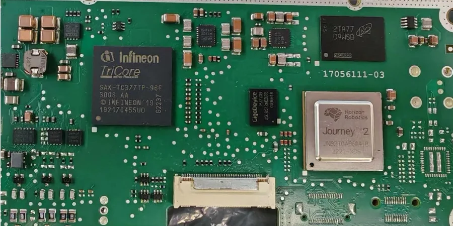
Flying probe test for ADAS and EV PCB reliability is most valuable before teams commit a new automotive board to powered debugging, coating, or fixture investment. On domain controllers, BMS boards, inverters, and on-board chargers, early electrical screening is where subtle shorts, wrong passives, rail leakage, and assembly escapes are cheaper to fix than to diagnose later.
That is why flying probe is still a critical method in prototype and small-batch builds. It gives automotive teams a fixtureless way to verify rail isolation, component integrity, high-speed support circuits, and high-voltage safety checkpoints before the board moves into a more expensive validation stage.
Why Flying Probe Test Matters for ADAS and EV PCB Reliability
ADAS and EV boards combine dense digital logic, sensitive analog monitoring, and high-current or high-voltage power sections on the same assembly. That mix creates several risks at once:
- Prototype revisions change fast, so dedicated ICT fixtures are expensive to update.
- Rail-to-rail leakage or a misplaced passive can destroy PMIC, SoC, BMS, or gate-driver sections at first power-on.
- GMSL, FPD-Link, and Automotive Ethernet support circuits still need electrical screening even when final signal-integrity validation happens later.
- High-voltage and high-current sections need isolation and low-resistance confirmation before environmental or functional testing.
- Coating, potting, and volume fixture planning should happen after the prototype is electrically clean, not before.
For that reason, many teams pair flying probe with prototype PCB assembly for automotive validation builds so they can move from fabrication to electrical screening without waiting on dedicated fixtures.
Key Reference Table for Flying Probe Test on ADAS and EV Boards
| Check item | Typical review window | Why it matters |
|---|---|---|
| Rail-to-rail and rail-to-ground isolation | Before first power-on of domain controller, BMS, inverter, or OBC boards | Prevents destructive shorts and unexpected leakage on critical power networks |
| Passive population and value checks | Decoupling networks, fuses, shunts, inductors, and termination components | Catches wrong-value or wrong-location parts before debug time is wasted |
| Differential-link support checks | GMSL, FPD-Link, and Automotive Ethernet support circuits | Screens termination, ESD paths, and basic symmetry issues before lab SI work |
| Low-resistance current-path measurement | High-current paths on EV power boards | Confirms copper path continuity and detects abnormal milliohm-level loss points |
| Hipot and isolation validation | High-voltage sections with required safety spacing | Verifies leakage behavior before HV functional test or environmental stress |
| Release gate before coating or potting | Assemblies entering protective finishing | Avoids sealing electrical defects into the finished product |
The exact limits still depend on the board architecture, component set, safety target, and customer validation plan, but this table defines the minimum review mindset for most ADAS and EV prototype builds.
Power Rail Isolation and Passive Checks Before First Power-On
On ADAS domain controllers and EV power boards, first power-on is often the most expensive moment to discover a basic assembly defect. A short between adjacent rails, an open fuse path, or the wrong inductor value can stop bring-up immediately and sometimes damage expensive silicon.
Flying probe helps reduce that risk by checking:
- Resistance between each critical rail and ground.
- Isolation between adjacent or redundant power rails.
- Presence and polarity of key passive and protection components.
- Continuity through fuse, shunt, filter, and sensing paths.
- Suspicious opens near hidden joints or dense packages that optical methods may not prove electrically.
This is especially useful on mixed-control and power products where one board includes PMIC sections, sensing circuits, gate drivers, and communications interfaces in the same build.
High-Speed Links, ESD Protection, and Termination Verification
ADAS camera, radar, LiDAR, and display boards depend on stable support circuitry around high-speed links. Flying probe is not a substitute for a full signal-integrity lab workflow, but it is a practical screen for the mistakes that commonly break those links before SI testing even starts.
Review points usually include:
- Differential-pair support symmetry through comparative resistance or capacitance measurements
- Termination resistor presence and value at the correct location
- ESD and TVS device connectivity on exposed interfaces
- Continuity across connectors, common-mode chokes, filters, and link-support networks
When the board stackup also depends on controlled impedance and dense escape routing, this screening works best alongside high-speed PCB material and impedance planning and HDI PCB fabrication for fine-pitch automotive layouts.
High-Voltage Safety, Low-Resistance Paths, and Thermal Monitoring
EV inverter, OBC, and battery-related boards add a second validation problem: electrical correctness alone is not enough unless the board also supports safe high-voltage spacing and predictable current flow.
Flying probe programs are commonly used to review:
- Hipot or insulation behavior between HV nets and low-voltage domains where the product architecture allows it.
- Milliohm-level continuity on high-current paths using Kelvin-style measurement methods.
- Thermistor, temperature-sense, and fault-feedback networks tied to thermal protection logic.
- Driver-circuit integrity for MOSFET or IGBT control sections.
For assemblies that combine thick copper paths, press-fit or through-hole power connectors, and mixed SMT/THT content, this work usually aligns with heavy copper PCB manufacturing for EV power stages and a controlled turnkey assembly process for automotive electronics.
How Flying Probe Complements SPI, AOI, X-Ray, and Fixture Strategy
The strongest automotive prototype flow is not based on a single inspection method. Flying probe works best when it closes the gap between visual inspection and the future production test plan.
In practice, the sequence often looks like this:
- Use SPI, AOI, and X-ray inspection for automotive ADAS and EV power assemblies to control solder-printing, placement, and hidden-joint workmanship.
- Use flying probe to verify electrical continuity, passive values, isolation behavior, and accessible support circuits.
- Review Boundary-Scan/JTAG strategy for automotive ADAS and EV power boards when digital devices need deeper interconnect validation.
- Convert stable, repeatable programs into ICT/FCT fixture planning for automotive ADAS and EV power production once the design is mature enough for volume tooling.
That staged approach keeps prototype coverage flexible while still preparing for a scalable production-release path.
When to Test Before Conformal Coating or Potting
Protective finishing makes electrical escape issues more expensive. Once an assembly is coated or encapsulated, rework becomes slower, riskier, or impossible on some automotive products.
That is why flying probe should be treated as a release gate before any harsh-environment finishing step. Teams that expect moisture, salt fog, vibration, or chemical exposure often review flying probe together with conformal coating strategy for automotive ADAS and EV power electronics and with workmanship criteria such as IPC Class 3 PCB manufacturing practices.
If BGA or bottom-terminated devices are part of the assembly, it is also worth pairing the release decision with SPI, AOI, and X-ray inspection for automotive ADAS and EV power PCB.
Common Questions
Is flying probe enough by itself for automotive PCB validation?
No. It is a strong structural and electrical screen for prototypes, but it still needs to sit beside optical inspection, X-ray where required, and functional or safety validation based on the product architecture.
Can flying probe measure controlled impedance directly?
Not in the same way as a TDR or VNA workflow. Its value is early screening of support circuits, symmetry indicators, termination networks, and obvious electrical escapes before formal SI characterization.
Which defects are most commonly found first with flying probe?
Rail shorts, unexpected leakage, wrong passive values, open fuse or shunt paths, connector continuity issues, and electrical faults that look visually acceptable but fail when measured.
When should a team move from flying probe to ICT or FCT fixtures?
Usually after the design, BOM, and test coverage are stable enough that fixture NRE and maintenance cost make sense for volume production.
Next Steps
If your ADAS or EV board is approaching prototype assembly, HV safety review, or pre-coating release, request a manufacturing review or contact the HILPCB engineering team. It is cheaper to fix isolation, passive, and coverage problems before powered debugging and fixture development start in parallel.
Related Reading
- Flying probe test for automotive ADAS and EV power prototypes
- SPI, AOI, and X-ray inspection for automotive ADAS and EV power assemblies
- Boundary-Scan/JTAG for automotive ADAS and EV power boards
- ICT/FCT fixture design for automotive ADAS and EV power production
- Conformal coating strategy for automotive ADAS and EV power electronics