
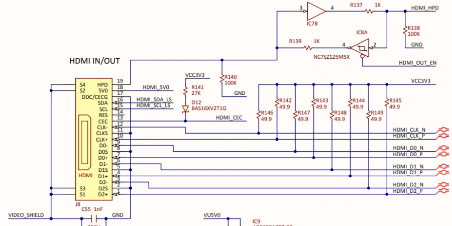
HDMI PCB design rarely fails because of a single routing mistake. In practice, most HDMI 2.0 and HDMI 2.1 FRL issues originate from early design decisions—stackup definition, reference plane strategy, connector footprint selection, and how well the design aligns with real manufacturing capabilities. Once these decisions are locked, later layout “fixes” offer limited leverage.
This article takes a production-first approach to HDMI PCB design, focusing on decisions that directly affect signal margin, yield stability, and compliance risk. The guide is organized into seven practical topics, each reflecting common failure points observed during prototype bring-up and volume production, with the goal of improving first-pass success for HDMI 2.0 and HDMI 2.1 FRL designs.
HDMI 2.0 vs HDMI 2.1 (TMDS vs FRL): What the PCB Must Handle
HDMI requirements change significantly with data rate. HDMI 2.0 (TMDS) is more tolerant of discontinuities than HDMI 2.1 FRL, where higher-frequency content makes the channel far more sensitive to via stubs, connector launches, and loss.
At HILPCB, we recommend locking the target mode early (2.0 TMDS or 2.1 FRL) and planning stackup + via strategy around real channel margin, not only routing convenience.
Key HDMI Performance Planning Techniques
- Define the target link mode early: HDMI 2.0 TMDS vs HDMI 2.1 FRL changes loss and discontinuity sensitivity.
- Budget routing length and transitions: long internal routes and frequent layer changes reduce margin faster at FRL rates.
- Treat connector launch as a design feature: pad/antipad geometry, via fields, and reference planes can dominate reflections.
- Decide verification requirements up front: controlled-impedance notes, impedance coupons, and reporting expectations.
Consistent Performance and Reliability
Designing with FRL-level discipline from the start improves interoperability across different cables and sinks, reduces respins, and makes compliance testing more predictable—especially for multi-port HDMI products.
100Ω Differential Impedance Planning: Make It Manufacturable, Not Fragile
HDMI high-speed lanes are typically designed around 100Ω differential impedance, but impedance is not “a single trace width.” It is the outcome of stackup, copper thickness, etch variation, solder mask effects, and how consistently the board is built.
At HILPCB, we aim for impedance geometry that is stable within typical fabrication tolerances—because a design that only works “at nominal” is a high-risk design. For tighter impedance repeatability and high-speed process control, many HDMI programs choose high-speed PCB fabrication capabilities as the baseline.
Key Impedance Control Techniques
- Start from stackup, not routing: choose dielectric thickness and copper weight so 100Ω is achievable without extreme line/space.
- Account for finished copper: plating and final copper thickness shift impedance.
- Keep a clean reference: route HDMI pairs adjacent to continuous ground planes (planned microstrip or stripline).
- Design to the center of tolerance: avoid “minimum-capability” geometry that drifts with normal variation.
- Choose processes aligned to high-speed builds: if margin is tight, high-speed capable fabrication reduces variability.
Consistent Performance and Reliability
Manufacturable 100Ω geometry improves lot-to-lot consistency and reduces field sensitivity to cable quality, sink tolerance, and environment changes.
HDMI Stackup Selection (4-Layer vs 6-Layer vs 8-Layer): SI and EMI First
Stackup defines impedance stability, return-path cleanliness, crosstalk risk, and routing feasibility. Many later-stage HDMI issues trace back to an early stackup that forced compromises: plane splits under pairs, noisy return paths, or too many transitions.
At HILPCB, we focus on stackups that keep HDMI referenced to solid planes and minimize transitions, especially for HDMI 2.1 FRL designs.
Key Stackup Planning Techniques
- 4-layer: best for simple, short routes (single port, lower density, limited high-speed coexistence). For cost-driven builds, a stable FR-4 PCB build is often the starting point.
- 6-layer: a strong default for professional designs—enables internal stripline routing with stable reference planes.
- 8-layer+: useful for multi-port, dense SoC/FPGA systems, strict EMC, or high routing congestion.
- Reserve HDMI routing corridors: avoid forcing pairs through noisy power areas or congested breakout regions.
- Choose the right structure for routing freedom: when density grows, moving to multilayer PCB manufacturing improves plane control and isolation options.
Consistent Performance and Reliability
A well-planned 6–8 layer structure improves isolation, lowers EMI risk, and increases first-pass success across prototypes and production.

HDMI Differential Pair Routing Rules: Geometry, Symmetry, and Crosstalk Control
Good routing discipline prevents reflections, crosstalk-induced sparkles, and mode conversion. The goal is predictable differential behavior from connector to IC.
At HILPCB, we treat differential routing as geometry management: constant width/spacing, continuous reference, and symmetry across P/N—especially through transitions.
Key Differential Routing Techniques
- Maintain constant geometry: keep width/spacing stable; avoid unnecessary neck-downs.
- Avoid sharp corners: use 45° bends or smooth arcs to reduce discontinuities.
- Keep separation between different pairs: reduce long parallel runs to limit crosstalk.
- Never cross plane splits: keep uninterrupted reference plane under the entire route.
- Use matching structures carefully: avoid aggressive “accordion” patterns that increase coupling and loss.
Consistent Performance and Reliability
Disciplined routing improves interoperability across different sinks/cables and reduces intermittent failures under temperature/voltage variation.
HDMI Length Matching and Skew Control: Practical Targets for 2.0 and 2.1
Length matching controls skew and helps preserve eye opening. HDMI 2.1 FRL generally needs tighter matching than HDMI 2.0. The key is to match intelligently: preserve symmetry and include transitions in your length accounting.
At HILPCB, we recommend setting constraints early in CAD rules and checking the final electrical path (including vias), not only visible trace length.
Key Length Control Techniques
- Intra-pair skew (P vs N): keep very tight; treat FRL designs as “high sensitivity.”
- Inter-pair matching: keep lanes aligned per your chipset guidance to avoid a “long lane” bottleneck.
- Use smooth serpentines: keep matching sections on the same layer and away from noisy regions.
- Include vias in measurement: layer transitions change electrical length and can create mismatch if ignored.
- Keep matching symmetric: avoid adding length only to one side of a pair.
Consistent Performance and Reliability
Good skew control increases margin and reduces the chance of “works in the lab but fails in customer setups.”
Via Transitions and Return Paths: Minimize Discontinuities and Control Stubs
At HDMI speeds, vias can become dominant discontinuities—especially if via stubs resonate inside the channel. Return-path discontinuities around layer changes can increase common-mode noise and EMI risk.
At HILPCB, we prioritize “transition hygiene”: reduce transitions, keep return paths continuous with nearby stitching vias, and control stubs when board thickness and FRL requirements demand it. For dense fanout near retimers/SoCs or tight connector escape, HDI PCB technology is often used to shorten stubs and improve routing quality.
Key Via and Return-Path Techniques
- Minimize layer transitions: keep HDMI pairs on one planned layer when possible.
- Place ground stitching vias near signal vias: preserve a tight return path through transitions.
- Keep via structures consistent across lanes: mismatched via geometry creates lane-to-lane differences.
- Manage stubs: thick boards or tight FRL margin may benefit from stub reduction strategies (build-dependent).
- Use advanced structures when density requires: HDI-style breakout can reduce detours and improve transition quality.
Consistent Performance and Reliability
Clean transitions reduce reflections and mode conversion, improve eye margin, and lower EMI surprises late in validation.
HDMI Connector + ESD Layout: Placement Rules That Prevent Field Failures
Many HDMI failures are driven by connector/ESD layout, not routing (our HDMI ESD protection guide covers TVS selection in detail): TVS too far away, inductive ground return, or shield grounding that forces ESD current into sensitive signal ground.
At HILPCB, we use a connector-first placement flow: lock connector + protection + discharge path first, then route HDMI pairs through that controlled structure. For a manufacturing-focused overview of controlled impedance, stackup execution, and assembly considerations, refer to this HDMI PCB fabrication & PCBA guide.
Key Connector and ESD Layout Techniques
- Place TVS arrays right at the connector: minimize unprotected trace length.
- Route in the correct order: Connector → TVS → IC (avoid bypass paths).
- Use multiple ground vias at TVS ground: low inductance is the real performance factor.
- Keep shield grounding low-impedance: solid grounding strategy improves both ESD robustness and EMI behavior.
- Choose stable build options for connector stress: for connector-heavy assemblies and repeated rework, high-Tg PCB materials can improve dimensional stability.
Consistent Performance and Reliability
A clean connector region—with correct protection placement and a true low-inductance discharge path—reduces catastrophic ESD damage and latent field degradation, while improving EMI robustness in real installations. For consistent placement of small TVS arrays and fine-pitch components, many teams pair the design with controlled SMT assembly services. If you prefer one supplier to manage PCB + parts + assembly delivery, turnkey assembly can reduce schedule risk and improve accountability.
Common Questions
What causes the most HDMI field failures?
Many failures come from connector and ESD-region layout mistakes such as TVS devices placed too far away, inductive ground return paths, or broken return-path continuity at layer changes. The interface region often matters more than trace length alone.
Do HDMI differential pairs always need perfect length matching?
Length matching matters, but impedance continuity, intra-pair skew control, reference-plane continuity, and clean via transitions matter just as much. Blindly forcing exact length without respecting the link budget does not guarantee a better channel.
When is HDI or high-Tg material worth using in an HDMI design?
They become valuable when connector escape is dense, stub reduction matters, the board may see repeated rework, or dimensional stability is critical. In those cases, the material and structure help create a more repeatable manufacturing window.