
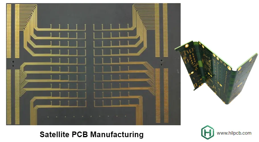
- A satellite integration PCB should be reviewed as an RF, thermal, and reliability platform for NTN or space hardware, not as a terrestrial telecom board with harsher branding.
- The first engineering checks are mission environment, operating band, low-outgassing material fit, thermal path in vacuum, radiation assumptions, and assembly survivability.
- NTN and satellite hardware force tighter decisions around material behavior, cleanliness, thermal conduction, and long-term stability than most ground-network PCB programs.
- Most failures come from using the wrong laminate family, ignoring outgassing and cleanliness rules, underplanning heat extraction in vacuum, or releasing hardware without a realistic environmental validation path.
- Early success usually depends on freezing mission profile, material family, thermal strategy, and validation sequence before the first prototype build.
A satellite integration PCB is the board or board set used in satellite payloads, gateway hardware, or NTN-supporting radio systems where RF performance, thermal control, cleanliness, and long-term reliability have to be managed under much stricter environmental assumptions than standard terrestrial electronics. The practical question is how to build a board that remains electrically and mechanically stable under vacuum, temperature cycling, and mission-specific reliability constraints.
Contents
- What to review first on a satellite integration PCB
- Key design and validation rule table
- Early engineering trade-off table
- How NTN and RF requirements affect material and stackup choice
- How outgassing, thermal control, and environment affect the board
- What prototype and assembly teams should freeze before release
- FAQ
- Next steps
- References
- Author and review
What to review first on a satellite integration PCB
Satellite hardware should not be evaluated with the same default assumptions used for ground telecom hardware. 3GPP Release 17 introduced formal 5G support for Non-Terrestrial Networks, while NASA and ECSS materials make it clear that vacuum, outgassing, and environmental control change how materials and assemblies must be judged.The first review points are usually:
- whether the hardware is for spaceflight, ground gateway, or NTN terminal use and what environment actually applies
- whether the intended RF band and signal path justify specialty laminate, hybrid stackup, or ceramic-adjacent solutions
- whether low-outgassing and cleanliness requirements are being applied at the material and assembly level
- whether the thermal path works under conduction and radiation assumptions rather than under terrestrial convection assumptions
- whether the design release includes a realistic environmental validation route for temperature, vibration, and mission-specific reliability
For satellite and NTN layouts, it is usually worth aligning high-frequency PCB, Rogers PCB, ceramic PCB, and high-thermal PCB assumptions before release.
Key design and validation rule table
| Rule / parameter | What to check first | Why it matters | How to verify | If ignored | | --- | --- | --- | --- | --- | | Mission environment | Freeze whether the board is for space, gateway, or terminal use | Environment determines what material, assembly, and test assumptions are valid | Program requirements review | Wrong validation path and poor reliability fit | | Material and stackup fit | Choose laminate and stackup by band, stability, and environment | RF performance alone is not enough in space-related hardware | Stackup review and materials review | Drift, contamination, poor long-run reliability | | Outgassing control | Check whether materials and processes align with low-outgassing expectations | Contamination risk can damage sensitive assemblies in vacuum environments | Material documentation and cleanliness review | Optical or reliability degradation | | Thermal path | Review conduction and radiation path early | Space hardware cannot assume fan-based cooling | Thermal review and enclosure contact review | Hotspots and unstable performance | | Radiation assumptions | Define what environment the electronics must survive | Radiation tolerance depends on the real program, not on generic telecom assumptions | System requirements review | Wrong part or shielding choice | | Environmental validation path | Freeze vibration, thermal, and cleanliness checks before build | Mission hardware is hard to salvage after late discovery | Validation plan review and pilot checklist | Delayed qualification and unclear failure modes |Early engineering trade-off table
| Design choice | Usually stronger for | Main trade-off | What to confirm early | | --- | --- | --- | --- | | Hybrid RF laminate stackup | Balancing RF loss and manufacturability | Material handling and lamination become more demanding | Band target and environment class | | Ceramic or ceramic-adjacent solution | Better thermal and dimensional stability in some paths | Higher cost and process constraints | Whether the mission really needs it | | Standard terrestrial assembly route | Lower cost and faster iteration | Often inadequate for stricter cleanliness and environment rules | End-use environment and contamination sensitivity | | Space-aware cleanliness and process control | Better fit for vacuum-sensitive hardware | Higher process discipline and documentation burden | Program requirements and verification scope | | Copper-heavy thermal spreading | Better conduction away from hotspots | Can complicate RF and weight constraints | Power map, weight budget, mechanical interface | | Integrated dense board set | Tighter packaging and shorter interconnect | Harder thermal and inspection path | Serviceability and heat extraction |How NTN and RF requirements affect material and stackup choice
NTN hardware is not defined by "6G" language alone. The real questions are operating band, signal path, environmental assumptions, and whether the board is in space, on the ground, or in a terminal. 3GPP Release 17 gives the standards context for NTN support, but the PCB consequences still depend on the actual hardware role.Three material and stackup decisions usually matter most.
1. Choose laminate by both RF need and environmental fit
Low-loss material may be necessary, but it is not sufficient by itself. The board also has to survive the real thermal and mechanical environment. That is why specialty material selection should be tied to both RF loss and mission constraints.
2. Review hybrid constructions as a manufacturing problem, not only a schematic choice
Hybrid stackups can make good sense, but they increase fabrication sensitivity. If the lamination plan, impedance plan, and environment assumptions are not aligned early, the board becomes harder to qualify. A Gerber viewer and PCB viewer review is often useful for checking where RF and thermal requirements collide physically.
3. Keep the validation path attached to the stackup choice
The board is not ready because the stackup looks plausible. It is ready when the stackup, materials, and environmental checks form one coherent release package.
How outgassing, thermal control, and environment affect the board
NASA's outgassing resources and ECSS materials both make the same practical point: contamination and thermal control are not secondary issues for space-oriented hardware. In a vacuum-related environment, material behavior that looks harmless on terrestrial electronics can create a real mission risk.The main engineering checks are:
- whether laminate, adhesive, coating, and assembly materials match the required outgassing and cleanliness expectations
- whether the thermal strategy is based on conduction and radiation rather than on assumed airflow
- whether high-power RF or conversion regions have a defined path into structure, spreader, or dedicated thermal features
- whether environmental validation includes the actual mix of vibration, cycling, and contamination-sensitive checks required by the program
If the design combines specialty material handling, dense RF routing, and controlled assembly requirements, SMT assembly, turnkey assembly, and PCB prototype planning usually needs to be reviewed as one workflow rather than split across teams.
What prototype and assembly teams should freeze before release
Satellite and NTN board risk usually drops when the release package is built around mission assumptions instead of generic telecom habits.A practical release checklist usually includes:
- Mission profile approved
Freeze whether the board is for orbital, gateway, or terminal use and what environment rules apply. - Material and stackup approved
Confirm laminate family, RF path rules, and thermal strategy against both band target and environment. - Outgassing and cleanliness route documented
Define the material-control and process-control expectations before procurement and assembly. - Thermal strategy completed
Confirm how heat moves into structure, spreaders, or other thermal interfaces under vacuum-relevant assumptions. - Environmental validation plan completed
Define the vibration, thermal, and reliability checks required for the first build stage. - BOM review completed
Use a BOM viewer review to catch specialty laminate, coating, connector, and thermal-interface sourcing risk before build release.
If the mission assumptions are still moving, quick-turn PCB support is usually better than locking a premature qualification build.
FAQ
Is a satellite integration PCB just a high-end telecom PCB?
No. Space and NTN-related hardware often adds stricter assumptions around outgassing, thermal control, cleanliness, reliability, and validation that do not apply in the same way to ordinary terrestrial telecom hardware.
Why is low outgassing such a big issue?
Because in vacuum-related environments, volatile material release can contaminate sensitive assemblies and create long-term reliability problems.
Does every NTN-related board need space-grade materials?
No. Gateway and terminal hardware may have very different requirements from orbital hardware. The right material choice depends on the actual environment and mission role.
Why is thermal design different for satellite hardware?
Because the board cannot assume ordinary air-cooling behavior. Heat usually has to move by conduction and radiation through a constrained structure.
What should be frozen first before prototype release?
Usually the mission environment, material family, outgassing route, and thermal strategy.
Next steps
If you are developing NTN or satellite-supporting hardware, the most useful next step is usually to review mission environment, material selection, outgassing control, and thermal path together before releasing the first prototype.HILPCB can support that process through:
- High-frequency PCB, Rogers PCB, and ceramic PCB planning for RF and environment-sensitive builds
- High-thermal PCB support when conduction path and heat extraction are major constraints
- SMT assembly and turnkey assembly coordination when specialty material handling and controlled assembly need one owner
- PCB prototype, quick-turn PCB, Gerber viewer, and PCB viewer for early validation
- Request a quote when your mission profile, material set, and assembly notes are ready