
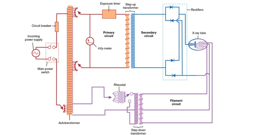
In X-ray PCB inspection systems, the filament circuit is the starting point of everything. It heats the X-ray tube filament, releases electrons, and ultimately determines how many X-ray photons are available to see inside solder joints, vias, and internal PCB layers. If the filament circuit is unstable, oversized, or poorly controlled, image quality, tube life, and inspection throughput all suffer.
This guide explains how the filament circuit in an X-ray tube works, which electrical and thermal parameters matter most, why X-ray inspection has become essential for advanced PCB technologies, and how to integrate filament-based inspection into a robust production workflow for both prototypes and high-volume manufacturing.
1. Understanding the Filament Circuit in an X-Ray Tube
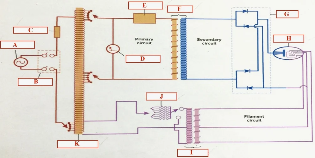
The filament circuit is a dedicated low-voltage, high-current subcircuit that powers the cathode filament inside the X-ray tube. When current passes through the filament, it heats to a very high temperature and emits electrons by thermionic emission. These electrons are then accelerated across a high-voltage field toward the anode target, where their impact generates X-ray photons.
In PCB inspection, filament circuit performance directly affects:
- X-ray intensity and image brightness
- Contrast between copper, solder, and substrate materials
- Ability to resolve microvoids, microcracks, and fine interconnects
- Tube thermal load and long-term reliability
A well-designed filament circuit allows precise control over tube current (mA) and supports a wide range of inspection modes, from low-power fine-detail imaging on small FR4 PCBs to higher-power penetration for thick or high-density assemblies.
Key Functional Elements of the Filament Circuit
Step-Down Power Stage
Converts higher system voltage into a few volts at several amps or tens of amps to heat the filament safely and efficiently.Current Regulation Loop
Ensures that the filament current, and therefore electron emission, follows the setpoint required for each imaging mode or X-ray protocol.Monitoring and Protection
Tracks filament current and voltage, detects overcurrent or short conditions, and integrates with system interlocks to prevent tube damage.Control Interface
Links the filament circuit to the X-ray system controller so that tube current can be coupled to exposure time, tube voltage, and detector settings for repeatable imaging.
By treating the filament circuit as a carefully controlled power supply rather than a simple heater, engineers can achieve stable X-ray output and reduce variability in PCB inspection results.
2. Filament Circuit Design Parameters for Stable X-Ray Output
Designing a filament circuit for an X-ray inspection system requires balancing electrical performance, response time, and tube protection. The goal is to deliver just enough heating current to achieve the desired tube current without overstressing the filament or causing image instability.
Key Electrical Design Considerations
Filament Voltage and Current Range
The circuit must support the filament’s full operating range, from low-current standby or “preheat” levels to higher currents used for maximum tube output.Current Control Accuracy and Stability
Precise control is needed because small changes in filament temperature can cause large changes in electron emission. Poor regulation leads to fluctuating image intensity and repeatability issues.Response Time and Ramp Profiles
Some systems preheat the filament and then ramp current when exposure starts. The circuit must respond quickly enough for production takt times while avoiding thermal shock to the filament.Isolation and Safety
Since the filament is often at high potential relative to system ground, the circuit may require galvanic isolation, robust insulation, and careful layout to meet safety standards.
Coordination with X-Ray Imaging Parameters
A filament circuit does not operate in isolation; it must be tightly integrated with:
- Tube high voltage (kV) – Higher voltage increases X-ray penetration, but filament current must adjust to maintain target tube current.
- Exposure time and frame rate – Short, frequent exposures may favor fast filament control; long static exposures demand stable thermal behavior.
- Detector gain and integration – Detector settings must complement filament output to avoid saturation while preserving contrast.
In PCB inspection systems designed for complex multilayer PCBs and dense interconnects, consistent filament circuit performance is crucial for automated defect recognition and process control.
3. Materials, Thermal Management, and Filament Lifetime
Because the filament operates at extreme temperatures, materials and thermal management strongly influence tube life, stability, and maintenance intervals.
Filament Materials and Structure
Tungsten Filaments
Tungsten is widely used thanks to its very high melting point, good mechanical strength at elevated temperatures, and favorable thermionic emission properties. It can sustain temperatures above 2,000 °C, which are needed to generate sufficient electron flow.Focusing Cup Integration
The filament is typically mounted inside a metal focusing cup that shapes the electron beam. The cup’s geometry and potential help concentrate electrons into a small focal spot on the anode, improving spatial resolution and image sharpness.
Thermal Management Strategies
Controlled Filament Loading
Operating at the lowest filament current that still achieves required image quality is one of the best ways to extend filament life. Constant high-output operation accelerates filament thinning and evaporation.Tube Cooling Systems
Air or liquid cooling keeps the tube envelope and anode temperature within limits. If cooling is insufficient, filament loading may need derating to avoid runaway thermal conditions.Load Curves and Derating
Manufacturers typically provide charts showing permissible combinations of kV, mA, and exposure time. Respecting these curves prevents overheating and early filament failure.
In systems used to inspect thermally demanding boards—such as power converters or LED drivers built on high-thermal PCBs—maintaining filament and tube health is essential to support continuous operation without frequent tube replacement.
4. Why Filament Circuit Based X-Ray Inspection Matters for Modern PCBs
As PCB technology has evolved, defects have become harder to see using only optical inspection or traditional test fixtures. The filament circuit, by powering high-resolution X-ray imaging, enables inspection of internal and hidden features that would otherwise go unchecked.
PCB Technology Trends Driving X-Ray Adoption
Higher Layer Counts and Density
Complex digital and mixed-signal designs now use dense routing on multilayer PCBs with blind and buried vias, via-in-pad, and stacked microvias that cannot be visually inspected.Temperature and Reliability Demands
Automotive, industrial, and power electronics often rely on high-TG PCBs to handle elevated temperatures and long service life, making inner-layer integrity and via quality more critical.Mechanical Flexibility
Wearables, foldable devices, and compact modules frequently use flex PCBs and rigid-flex constructions, where joints and traces may be hidden within bends, adhesives, or laminated sections.High-Speed and RF Performance
Networking, radar, and wireless systems use high-frequency PCBs that demand tight impedance and clean internal structures; small internal defects can cause intermittent or frequency-dependent failures.
Defect Types X-Ray Can Reveal
With properly tuned filament circuit output and tube settings, X-ray inspection can reveal:
- Solder bridges between fine-pitch leads or BGA balls
- Voids in thermal pads and power pads
- Insufficient barrel fill in plated through holes
- Misaligned or missing inner-layer pads and via connections
- Crack propagation in solder joints after thermal cycling or vibration
- Delamination or internal damage in complex laminate stacks
As boards become more complex, filament-powered X-ray imaging has shifted from a “nice to have” tool to a core requirement in many high-reliability and high-density PCB production lines.
5. Core Architecture of an X-Ray PCB Inspection System
To appreciate how the filament circuit supports defect detection, it helps to understand the main subsystems in an X-ray PCB inspection machine and how they interact.
Main Subsystems
X-Ray Tube and Filament Circuit
The tube generates X-rays from electrons emitted by the filament. The filament circuit sets the electron emission level, while a high-voltage supply accelerates electrons toward the anode target.Mechanical Motion and Sample Handling
Motorized stages move PCBs in X, Y, and Z, and sometimes tilt, allowing different viewing angles on solder joints, vias, and internal features. This is important for large or complex boards, including RF and digital sections built on high-speed PCBs.Detector and Imaging Electronics
A flat-panel detector or image intensifier converts X-ray photons into digital images. Detector gain, integration time, and resolution must be coordinated with filament output to avoid noise or saturation.Control and Software
System control software links filament circuit setpoints, tube voltage, motion patterns, and image processing. Advanced systems offer automated defect recognition, measurement tools, and reporting for process control.
Impact of Filament Circuit on System Performance
- Consistent filament current yields stable image brightness and contrast.
- Proper filament control allows lower kV settings when possible, reducing tube stress while maintaining visibility of solder and copper.
- Optimized filament-drive profiles support fast inspection cycles without overshooting temperature limits.
In short, the filament circuit is not just a heater; it is a precision, high-current power subsystem that must be tightly integrated into the overall X-ray inspection architecture.
6. Integrating Filament Circuit Control into PCB Quality and Production Workflow
For electronics manufacturers, the real value of a filament circuit driven X-ray system comes when it is fully integrated into the PCB fabrication and assembly process, rather than used as an isolated laboratory tool.
Supporting SMT and Assembly Lines
X-ray inspection is commonly used alongside SMT assembly processes to:
- Check BGA, QFN, and hidden pad joints after reflow
- Evaluate stencil design, paste volume, and voiding levels
- Validate process changes, new materials, or new board revisions
Stable filament circuit settings, tied to product families and panel thicknesses, help standardize inspection recipes and reduce variability in pass/fail judgments.
From Prototypes to Volume Production
During early development, engineers often use X-ray inspection on prototypes and pre-series builds to debug layout decisions, via structures, and assembly parameters. As designs mature, X-ray results are correlated with other tests to define acceptance criteria and process limits.
Many teams ultimately rely on manufacturing partners that provide integrated turnkey assembly services, where PCB fabrication, assembly, X-ray inspection, and test are coordinated under one roof. In this model:
- Filament circuit parameters and X-ray recipes are documented as part of the production process.
- Results are used for statistical process control and continuous improvement.
- Tube health and filament life are monitored to plan maintenance without disrupting deliveries.
By treating the filament circuit as a critical, controllable part of the X-ray inspection ecosystem—and not just a background power stage—manufacturers can consistently detect hidden defects, protect reliability, and support the ever-increasing complexity of modern PCB technologies.
Common Questions
Why is the filament circuit so important in an X-ray PCB inspection system?
Because it determines how stably the X-ray tube emits electrons, which directly influences X-ray output, image clarity, and inspection repeatability. If that front-end source is unstable, downstream imaging performance usually suffers no matter how good the rest of the system is.
Which factors most directly affect image quality and tube life?
Filament current control, thermal stability, ramp-up behavior, and long-term load management all have a strong impact on both image quality and tube longevity. Overshoot, drift, or poor control strategy can shorten tube life while also reducing inspection consistency.
Why do manufacturers need ongoing calibration and monitoring of the filament loop?
Because drift in this kind of circuit often appears gradually and may not be visible in occasional spot checks. Recording parameters, watching trends, and planning maintenance proactively helps keep inspection quality repeatable over time.